| Nov 22, 2019 |
Graphene mapping in minutes instead of hours(Nanowerk News) If we want to be able to create new and innovative components of two-dimensional materials like graphene, we need tools to characterize their quality. Raman spectroscopy is the gold standard for this, but its major disadvantage is the low speed. Apart from that, the laser light can also damage some of the two-dimensional materials. University of Twente researchers added a smart algorithm to the detection, resulting in ‘Raman’ working at least fifty times faster and making it more ‘gentle’ to sensitive materials. |
| The research is presented in National Science Review ("Algorithm-induced high speed and non-invasive confocal Raman imaging of two-dimensional materials"). |
| Graphene is always raising high expectations, as a strong, ultrathin, two-dimensional material that could also be the basis for new components in information technology. There is huge need for characterization of graphene devices. |
| This can be done using Raman spectroscopy. Laser light is sent to the material sample, and inelastically scattered photons tell us about the rotations and vibrations of the molecules inside, and thus about the crystal structure. |
| On average, only around 1 in 10 million photons is scattered in this way. This not only makes it hard to detect the right information, it is also very slow: it may take half a second to image one single pixel. |
| The question is if Raman still remains the best option, or if there are better alternatives. UT researchers Sachin Nair and Jun Gao keep Raman spectroscopy as a starting point, but manage to improve the speed drastically: not by changing the technique itself, but by adding an algorithm. |
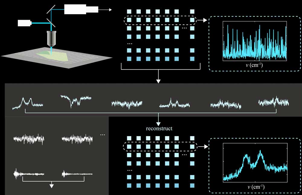 |
| Recovering the real signal from the noisy one, in Raman spectroscopy, leads to a 50 to 100 times higher mapping speed of materials like graphene. (click on image to enlarge) |
Recovering the real signal |
| This algorithm is not unknown in the world of signal processing and it is called Principal Component Analysis. It is used to improve the signal-to-noise ratio. PCA determines the characteristics of noise and those of the real signal. The larger the dataset, the more reliable this recognition is. |
| Apart from that, modern Raman instruments have a detector called electron-multiplying charge-coupled device (EMCCD) that improves the signal-to-noise-ratio. The net result of this work is that processing one pixel doesn’t take half a second, but only 10 milliseconds or less. An important feature for vulnerable materials like graphene oxide is that the intensity of the laser can be lowered. These are major steps ahead for getting a fast grip on the materials’ properties. |
Multi-purpose |
| Except for graphene, the improved Raman technique can also be used for other two dimensional materials like germanene, silicene, molybdenum disulfide, tungsten disulfide and boron nitride. Use of the algorithm is not limited to Raman spectroscopy; techniques like Atomic Force Microscopy and other hyperspectral techniques could also benefit from it. |
| The research has been done in the group Physics of Complex Fluids (PCF) of Prof Frieder Mugele, part of UT’s MESA+ Institute. The researchers collaborated with the Medical Cell BioPhysics group and the Physics of Interfaces and Nanomaterials group, both of the University of Twente as well. |
| Source: University of Twente |
|
Subscribe to a free copy of one of our daily Nanowerk Newsletter Email Digests with a compilation of all of the day's news. |

