| Mar 24, 2020 |
New metasurface helps make the switch to terahertz frequencies(Nanowerk News) Researchers are finding promising new applications for terahertz radiation (between microwaves and infrared light). Terahertz radiation could lead to new capabilities in imaging, wireless communications, and other areas. To expand its use, we need new devices designed for terahertz frequencies. Those needs include switches that work in less than a thousandth of a second, have a high contrast between “off” and “on” states, and efficiently carry electrical charges. |
| Researchers have developed a new metasurface –an artificial material only billionths of a meter thick—that does all three (Nano Letters, "Terahertz Detection with Perfectly-Absorbing Photoconductive Metasurface"). |
| The new highly efficient metasurface switch needs no metal or backing material. This means detectors using the switch would be smaller, thinner, more efficient, and require less power. That makes them lower in cost and easier to integrate into terahertz detectors for communications and imaging. Terahertz radiation has potential safety and other benefits compared to other frequencies. |
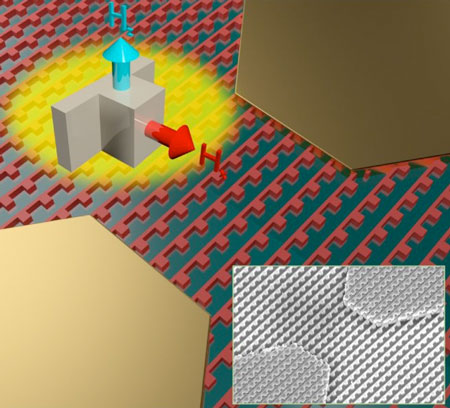 |
| Graphic depicting a photoconductive metasurface. Each unit cell supports resonance of light on two axes of symmetry (labeled Hx and Hz) to enable perfect light absorption. The inset image shows a scanning electron micrograph of a terahertz detector. (© ACS) |
| Terahertz radiation is in the band of frequencies higher than microwaves but lower than infra-red light. Terahertz radiation is very safe, and technologies such as wireless communications and imaging systems may eventually use this frequency range. Researchers are therefore developing devices that can efficiently generate, detect, and modulate terahertz waves. |
| A key technology for terahertz devices is an ultrafast photoconductive switch,a switch that would use light to change electrical conductivity between a highly resistive “off” state and a highly conductive “on” state in less than a picosecond (one trillionth of a second). |
| To achieve this performance, these switches need high contrast in conductivity between the “on” and “off” states. Until recently, researchers have not been able to meet this requirement. |
| Now, researchers at the Center for Integrated Nanotechnologies, a Department of Energy Nanoscale Science Research Center, have solved that challenge. The researchers developed a perfectly absorbing ultrathin photoconductive metasurface. |
| The metasurface is a network of tiny repeating structures called resonators. These connected resonators support magnetic dipole modes and can efficiently absorb light at a desired wavelength. They achieve perfect light absorption using two overlapping resonances with the correct symmetry. |
| The resulting metasurface is a tenth of the thickness of the original photoconductive switch. The thinner the device, the greater the contrast between “off” and “on” states. |
| The metasurface could be applied to applications such as efficient fast modulators, a critical component of modern communication systems, and smaller, more efficient terahertz detector arrays. |
| Source: Sandia National Laboratories |
|
Subscribe to a free copy of one of our daily Nanowerk Newsletter Email Digests with a compilation of all of the day's news. |

