| Apr 27, 2020 |
New study reveals how impurities affect the electrical properties in anisotropic 2D materials(Nanowerk News) The reduced symmetry in anisotropic two-dimensional (2D) materials gives rise to intrinsically inhomogeneous electrical, optical, thermal, and mechanical responses. As a result, these materials hold promises for the realization of novel angle-dependent devices, such as digital inverters, polarization-sensitive photodetectors and thermoelectric devices. |
| Nowadays, it should be possible to predict such properties with great detail. However, for the realization of advanced functional devices a detailed knowledge of the material´s intrinsic properties might not be enough. |
| Indeed, the intrinsic properties will be inevitably affected by the materials’ structural defects, such as vacancies and grain boundaries, as well as by external factors, like the presence of a substrate, metal contacts or surface contaminants. |
| At present, though, the impact of these impurities on the physical properties of anisotropic 2D materials remains largely unexplored. |
| In a study published in Physical Review Applied ("Impact of Impurities on the Electrical Conduction of Anisotropic Two-Dimensional Materials"), a team of researchers led by Dr. Luca Camilli at the University of Rome “Tor Vergata” (Italy) show how impurities affect the electrical properties in anisotropic germanium arsenide (GeAs). |
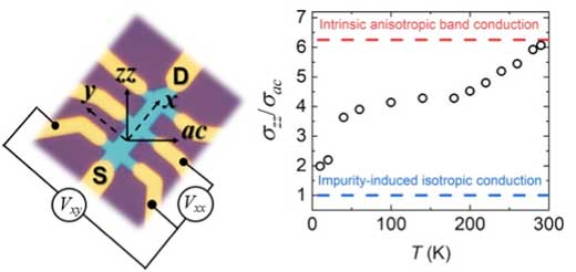 |
| Left: Image of a transistor with a few-layer GeAs channel. Right: Conductivity ratio as a function of temperature. (© Physical Review Applied) |
| In particular, they report that the ratio of conductivities along the armchair and zigzag crystallographic directions exhibits an unexpected dependence with respect to both temperature and carrier density. This behavior is directly related to the presence of impurity-induced localized states in the bandgap that introduce isotropic hopping conduction. |
| The effective electrical transport in GeAs can indeed be understood only by considering both the intrinsic anisotropic band conduction and the impurity-induced isotropic conduction. |
| Since factors such as structural defects, surface contamination, trapped states at the interface between 2D material and substrates are impossible to eliminate completely in electronic devices, the results presented in this study will be beneficial for future exploitation of anisotropic 2D materials in practical applications. |
| Source: Technical University of Denmark (DTU) |
|
Subscribe to a free copy of one of our daily Nanowerk Newsletter Email Digests with a compilation of all of the day's news. |

