| May 28, 2020 |
Photonic crystals: 'even thin is functional'(Nanowerk News) Photonic crystals are the nanostructures that can manipulate photons by means of an energy gap, similar to how the semiconductors in computer chips manipulate electronic current. It was always thought that photonic crystals should be thick and bulky to be functional. |
| Scientists from the University of Tokyo, the University of Electro-Communications in Tokyo, the Kyoto Institute of Technology and the University of Twente discovered that even very thin 3D photonic band gap crystals are powerful devices to strongly control the flow of light. |
| The new insights lead to design rules for new optoelectronic devices for efficient telecommunication and computers, and thin solar cells. |
| The resulting paper will appear in the journal Physical Review B ("Reflectivity of Finite 3D GaAs Photonic Band Gap Crystals") that is published by the American Physical Society. |
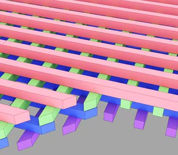 |
| Figure 1. Cartoon of the woodpile photonic crystal structure that has a similar structure as a diamond crystal (inset) but a thousand times magnified. (Image courtesy of the researchers) |
| “We studied carefully assembled photonic crystals with the so-called woodpile structure", says leading author Dr. Tajiri (see Fig. 1). "Our crystals consist of a stacked arrays of rods in two perpendicular directions in a semiconductor wafer such as gallium arsenide. The crystal structure is inspired by diamond gemstones.” |
| The advanced method conveniently allows making thin structures of only a few layers thick, between a few hundred nanometers to about one micron. |
Japanese-Dutch collaboration |
| To investigate their new crystals, the Japanese-Dutch team decided to measure the reflectivity spectra. Therefore, after fabrication in Japan, they were shipped to Twente for microscopic measurements. The spectra showed that the thin diamond-like photonic crystals function remarkably well: all crystals showed both a high reflectivity and broad peaks. Remarkably, this occurred even for the thinnest crystal. |
| The reflected light is forbidden to enter crystals over a considerable range of wavelengths, also known as a forbidden gap. In the Japanese-Dutch crystals, the situation is even more radical, since the light is forbidden to travel in all directions simultaneously. |
| Dr. Tajiri explains: “The quick formation of the forbidden gap in our crystals is remarkable because earlier 3D crystals required a large thickness for a gap to emerge.” |
Possible applications |
| Prof. Iwamoto leader of the Japanese team says: “Our discovery that even thin photonic crystals are powerful devices means that we can save considerable fabrication time and resources.” And prof. Vos, leader of the Dutch team, enthuses: “The result that even thin structures are fully functional is great news for applications in photovoltaics. Here, scientists are looking for thin broadband backreflectors to improve the performance of thin solar cells”. |
The team |
| The research has been performed by Dr. Takeyoshi Tajiri from the University of Electro-Communications, Chofu in Tokyo, Japan, Dr. Shun Takahashi from the Kyoto Institute of Technology, Prof. Yasuhiko Arakawa from Institute for Nano Quantum Information Electronics, Prof. Satoshi Iwamoto from the Institute of Industrial Science and the Research Center for Advanced Science and Technology at the University of Tokyo, and Cornelis Harteveld BSc and Prof. Willem Vos from the MESA+ Institute for Nanotechnology, University of Twente. The research project is supported by Japan Society for the Promotion of Science, KAKENHI, the Nederlandse Organisatie voor Wetenschappelijk Onderzoek; and MESA+ section Applied Nanophotonics. |
| Source: University of Twente |
|
Subscribe to a free copy of one of our daily Nanowerk Newsletter Email Digests with a compilation of all of the day's news. |

