| Jun 09, 2020 |
Harnessing light for nanotechnologies(Nanowerk News) Scientists found a new way to build silicon nanodisks - extremely tiny, flat, round objects. With this new technology, scientists can guide light along the outside of these tiny structures in a way they have never been able to before (Nature Nanotechnology, "Nonlinear light generation in topological nanostructures"). |
| Unlike in previous structures, they were able to send light in a zig-zag pattern rather than a straight line. |
| In addition, previous 2D structures were too big to use in nanoscale applications. Improving the ability to move the light in multiple dimensions will make it easier to integrate these nanostructures into technologies in the future. |
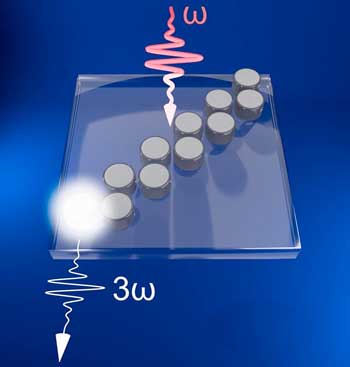 |
| Researchers guided photons through a zigzag design of silicon nanodisks, demonstrating the first fully three-dimensional (3D) nonlinear topological nanostructure for light generation. (Image: Oak Ridge National Laboratory) |
| Improving the efficiency and reducing the cost of several technologies require that scientists be able to manage light energy at the nanoscale. Previous technologies have only been able to generate light in straight lines and guide it in a single direction. |
| In addition, these larger structures are too big to use in nanoscale devices. But light-based energy systems that protect themselves against disorder and other influences that disrupt performance could help. |
| 3D nanostructures like those in this study could lead to smaller, faster, and more efficient nanotechnologies such as quantum computing, solar cells, and communications. |
| Managing photons, or light energy, at the nanoscale is an important route to improving the efficiency and reducing the cost of transformative energy technologies with broad applications ranging from solar cells to quantum computers. However, light generation has been limited to linear pathways, meaning it can only be guided in one direction, and macroscale structures that are not compatible with nanoscale devices. |
| Novel fabrication of 3D nanostructures that enable multi-directional light manipulation will open new territory for photon-based nanotechnologies that are smaller, faster, and more efficient than current resources. |
| One of the challenges of pushing photonics to more complex structures at the nanoscale is to overcome material defects and deformations that can disrupt signaling and result in energy loss or poor performance. New efforts to incorporate “topological” structures, configurations that are not altered by deformations like stretching or twisting, into light physics enable materials to be fine-tuned at the atomic level to enhance energy efficiency (e.g., photon signaling) and realize the full potential of photons in nanoscale devices. |
| Source: U.S. Department of Energy, Office of Science |
|
Subscribe to a free copy of one of our daily Nanowerk Newsletter Email Digests with a compilation of all of the day's news. |

