| Aug 27, 2020 |
Fabrication of a single-crystal giant magnetoresistive device on a polycrystalline film(Nanowerk News) NIMS and AIST have jointly succeeded in fabricating a giant magnetoresistive (GMR) device comprising single-crystal Heusler alloys on an practical silicon substrate (Acta Materialia, "Fully Epitaxial Giant Magnetoresistive Devices with Half-metallic Heusler Alloy Fabricated on Poly-Crystalline Electrode Using Three-Dimensional Integration Technology"). |
| The team demonstrated for the first time that a single-crystal magnetoresistive device can be bonded onto the surface of a polycrystalline electrode using a wafer bonding technique. The fabrication of high-performance single-crystal devices has proven challenging, and these results may provide new guidance in the development of larger capacity hard disk drives (HDDs). |
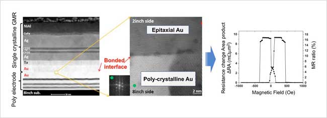 |
| Cross-sectional transmission electron micrographs of the bonded interface between the single-crystal GMR film device and the polycrystalline electrode wafer (two photos at left) and magnetoresistance measured in the device post-bonding (right). (Image: NIMS) (click on image to enlarge) |
| Some Heusler alloys (e.g., Co2MnSi) are known to possess half metallic property-substances that act as conductors to electrons of only one spin orientation when their atoms are in an orderly arrangement. In previous research, a high-quality GMR device was fabricated using half-metallic Heusler alloys. |
| This device was reported to exhibit an extremely large magnetoresistance ratio, a characteristic vital to the development of hard disk read heads compatible with HDDs with nearly five times the recording density of current HDDs. |
| However, the fabrication of this GMR device required the use of a heat-resistant single-crystal magnesium oxide (MgO) substrate with an appropriate lattice structure, which is considerably more costly than using the industrially established small MgO substrate. |
| In addition, HDD read heads need to be fabricated on a polycrystalline magnetic shield, despite the fact that it is impossible to grow a single-crystal device directly on the surface of a polycrystalline film with crystal grains having various lattice orientations. |
| Moreover, Heusler alloys have to be annealed at a temperature of at least 300 °C to form an orderly atomic ordering. However, this annealing process also damages the magnetic shield layer. |
| These issues have prevented practical applications of GMR devices comprising single-crystal Heusler alloys. |
| This research team deposited a NiAl/CoFe buffer layer on the surface of a conventional, inexpensive silicon substrate and discovered that the substrate acquired significantly increased heat resistance and a smoother surface. |
| The team then fabricated a GMR device comprising single-crystal Heusler alloys on the silicon substrate and confirmed that the device performs comparably to the GMR device grown on the MgO substrate. The team also grew a polycrystalline electrode film on the surface of another substrate and fabricated a GMR film device comprising single-crystal Heusler alloys on it. |
| The team subsequently bonded the fabricated GMR film device onto a wafer using the latest three-dimensional integration technology. Through these processes, the team formed an extremely smooth, defect-free bonded interface between the polycrystalline and single crystal films by optimizing wafer bonding conditions. |
| The team also confirmed that bonding the fabricated GMR film device onto a wafer did not negatively affect the device's magnetoresistive performance. |
| The techniques the team developed are expected to eliminate the need to grow a single-crystal magnetoresistive device directly on a polycrystalline electrode film and completely resolve the damage issue caused by high-temperature treatment. |
| These techniques are applicable not only to the fabrication of GMR devices comprising single-crystal Heusler alloys but also for various other purposes, such as the integration of single-crystal tunneling magnetoresistance devices--another potentially promising high-performance technology--onto a heat-susceptible circuit board. The use of these techniques may promote practical use of high-performance single-crystal spintronic devices, thereby potentially contributing to the development of larger capacity HDDs and magnetoresistive random access memory. |
| Source: National Institute for Materials Science, Japan |
|
Subscribe to a free copy of one of our daily Nanowerk Newsletter Email Digests with a compilation of all of the day's news. |

