| Oct 20, 2020 |
Integrated circuit of pure magnons(Nanowerk News) A team of physicists are marking a milestone in the quest for smaller and more energy-efficient computing: they developed an integrated circuit using magnetic material and magnons to transmit binary data, the 1s and 0s that form the foundation of today’s computers and smartphones. |
| The new circuit is extremely tiny, with a streamlined, 2D design that requires about 10 times less energy than the most advanced computer chips available today, which use CMOS technology. While the current magnon configuration is not as fast as CMOS, the successful demonstration can now be explored further for other applications, such as quantum or neuromorphic computing. |
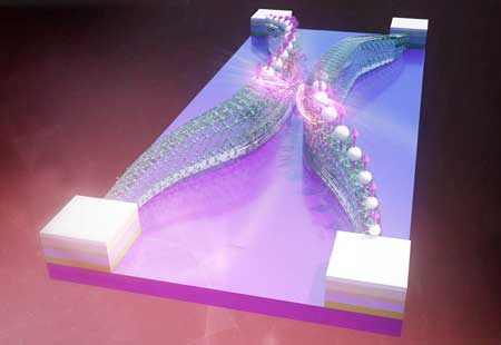 |
| The directional coupler with a visible atomic structure is depicted. Spin wave jumps from one nanowire conduit to another nanowire at the point where the conduits are getting closer one to another. (Image: Niels Paul Bethe, SYNC audiovisual design) |
Successful collaboration |
| The prototype is the culmination of four years of effort funded through Andrii Chumak’s European Research Council (ERC) Starting Grant, and close collaboration with Jun.-Prof. Dr. Philipp Pirro at TUK, and Dr. Qi Wang, who is currently a postdoc at University of Vienna. Univ.-Prof. Chumak started the work at TUK and now leads a research group at University of Vienna. |
| “We are very happy since we managed to do what was planned several years ago and it works even better than we expected,” Chumak says. When he first proposed the magnon circuit, his design was very complex. He credits Wang, the lead author of the paper (Nature Electronics, "A magnonic directional coupler for integrated magnonic half-adders"), with making the design “at least 100 times better.” “We see now that magnonics circuits can be as good as CMOS, but this is probably not yet enough if you want to trigger industry. I would assume you have to be still at least 100 times smaller and faster,” says Chumak. “But this circuit opens up fantastic opportunities beyond binary data, for example to quantum magnonic computing at very low temperatures.” Pirro adds: “We are also interested in adapting the circuit for neuromorphic magnonic computers inspired by the functionality of our brain.” |
How it works |
| The nanocircuit components measures less than one micrometer, far thinner than a human hair and hardly visible even under a microscope. It comprises of three nanowires made of a magnetic material called yttrium iron garnet. |
| The wires are positioned precisely in relationship to each other to create two “directional couplers,” which guide magnons through the wires. Magnons are quanta of spin waves – think of them like ripples on the surface of pond after throwing in a rock, but in this case, the waves are formed by distortions in the magnetic order of a solid material on the quantum level. It took a lot of time and effort to figure out the best nanowire length and spacing to generate the desired outcomes. |
| Wang worked on the project for his Ph.D. at TUK. “This is the 3rd or 4th design,” he says. “I ran a few hundred simulations for different types of half-adders.” |
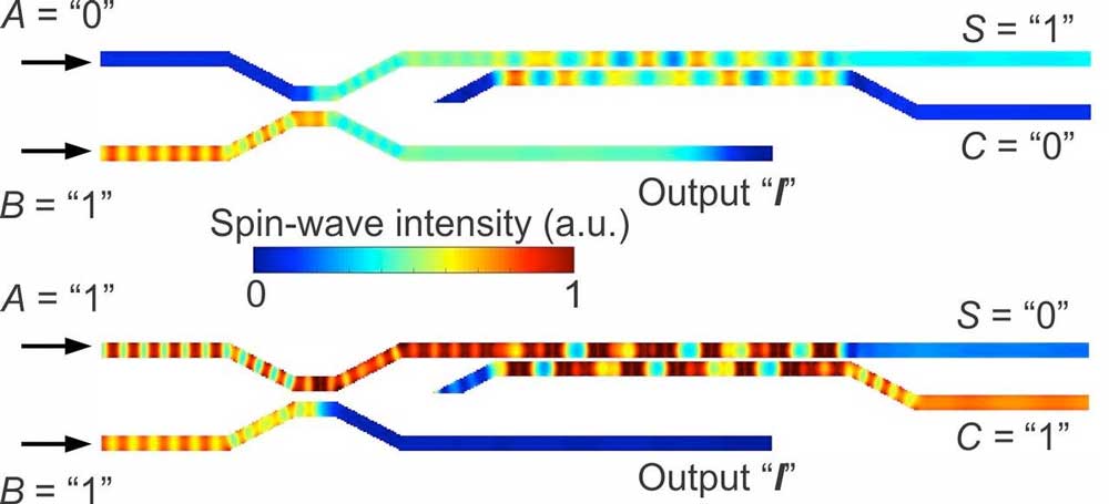 |
| The operational principle of the half-adder. The information is encoded into spin-wave intensity: red corresponds to logic “1”, blue to logic “0”. When only one of the inputs is „1“, the second directional coupler operates in a linear regime and the wave transmits towards the top output “S”. If both inputs have “1” signal, the directional coupler switches to the nonlinear regime and the output wave reaches the bottom “C” output. Any combination of the input signals satisfies the truth table of a half-adder. (Image: Qi Wang, University of Vienna) (click on image to enlarge) |
| At the first coupler, where two wires are very close together, the spin wave is split in half. One half proceeds to the second coupler, where it jumps back and forth between the wires. Depending on the amplitude, the wave will exit either the top or bottom wire, which corresponds to binary “1” or “0”, respectively. |
| Since the circuit contains two directional couplers that add together two streams of information, it forms a “half-adder,” one of the most universal components of computer chips. Millions of these circuits can be combined to conduct increasingly complex calculations and functions. |
| “What typically requires hundreds of components and 14 transistors in regular computers, here only requires three nanowires, a spin wave, and nonlinear physics,” Pirro says. |
Future applications |
| Pirro, who is currently leading the direction of spintronic computing at TUK in the frames of the collaborative research center “Spin+X”, will now explore using the magnon circuit for neuromorphic computing, which approaches data processing not as binary, but more like the human brain. |
| Spin waves are much better suited for the more complex systems and have the potential to carry a great deal more information because they have two parameters – amplitude, which is wave height, and phase, which is the wave angle. In the current demonstration, the team did not use phase as a variable in order to keep it simple for binary data processing. |
| “If this device can already compete with CMOS, even if it is not using the full power of the wave-based approach, then we can be quite confident a scheme using the full power of the spin wave can be more efficient than CMOS for certain tasks,” Pirro says. “And the ultimate goal, of course, is to combine the strengths of both CMOS and magnonics technologies together.” |
| Source: Technische Universität Kaiserslautern |
|
Subscribe to a free copy of one of our daily Nanowerk Newsletter Email Digests with a compilation of all of the day's news. |

