| Feb 03, 2021 |
Nanosheet-based electronics could be one drop away
(Nanowerk News) Scientists at Japan’s Nagoya University and the National Institute for Materials Science have found that a simple one-drop approach is cheaper and faster for tiling functional nanosheets together in a single layer. If the process, described in the journal ACS Nano ("Single Droplet Assembly for Two-Dimensional Nanosheet Tiling"), can be scaled up, it could advance development of next-generation oxide electronics.
|
|
“Drop casting is one of the most versatile and cost-effective methods for depositing nanomaterials on a solid surface,” says Nagoya University materials scientist Minoru Osada, the study’s corresponding author. “But it has serious drawbacks, one being the so-called coffee-ring effect: a pattern left by particles once the liquid they are in evaporates. We found, to our great surprise, that controlled convection by a pipette and a hotplate causes uniform deposition rather than the ring-like pattern, suggesting a new possibility for drop casting.”
|
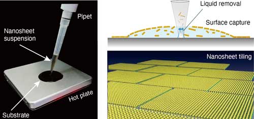 |
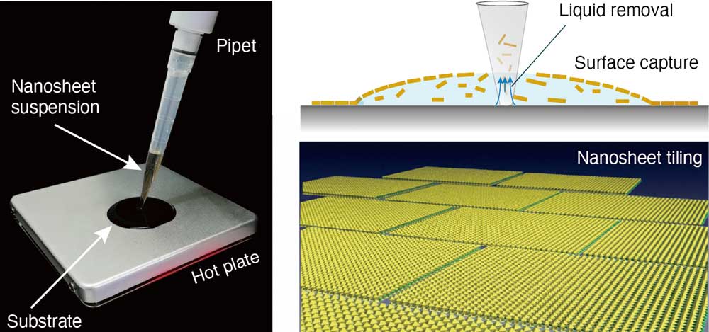
| The process, which involves dropping a nanosheet suspension onto a substrate heated by a hot plate and then removing the solution, leads to a uniform surface tension-driven tiling of the nanosheets, with limited gaps between them. (© ACS Nano) (click on image to enlarge)
|
|
The process Osada describes is surprisingly simple, especially when compared to currently available tiling techniques, which can be costly, time-consuming, and wasteful. The scientists found that dropping a solution containing 2D nanosheets with a simple pipette onto a substrate heated on a hotplate to a temperature of about 100°C, followed by removal of the solution, causes the nanosheets to come together in about 30 seconds to form a tile-like layer.
|
|
Analyses showed that the nanosheets were uniformly distributed over the substrate’s surface, with limited gaps. This is probably a result of surface tension driving how particles disperse, and the shape of the deposited droplet changing as the solution evaporates.
|
|
The scientists used the process to deposit particle solutions of titanium dioxide, calcium niobate, ruthenium oxide, and graphene oxide. They also tried different sizes and shapes of a variety of substrates, including silicon, silicon dioxide, quartz glass, and polyethylene terephthalate (PET). They found they could control the surface tension and evaporation rate of the solution by adding a small amount of ethanol.
|
|
Furthermore, the team successfully used this process to deposit multiple layers of tiled nanosheets, fabricating functional nanocoatings with various features: conducting, semiconducting, insulating, magnetic and photochromic.
|
|
“We expect that our solution-based process using 2D nanosheets will have a great impact on environmentally benign manufacturing and oxide electronics,” says Osada. This could lead to next-generation transparent and flexible electronics, optoelectronics, magnetoelectronics, and power harvesting devices.
|