| Aug 16, 2022 |
New van der Waals heterostructures for high-efficiency infrared photodetection
(Nanowerk News) Profs HU Weida and PENG Hailin, two of researchers at Shanghai Institute of Technical Physics and Peking University, recently proposed momentum-matching and band-alignment van der Waals heterostructures to solve the low QE of 2D materials infrared photodetectors.
|
|
The results were published in Science Advances ("Momentum-matching and band-alignment van der Waals heterostructures for high-efficiency infrared photodetection").
|
|
Infrared photodetectors with a high quantum efficiency (QE) can be used for ultraweak light detection and quantum communication. However, QE is largely limited by absorptivity and defect-recombination of infrared absorbers as well as the collection of the photogenerated carrier, which severely impedes the fabrication and further development of infrared photodetectors with a high QE. As a result, direct-bandgap semiconductors with a high photoelectric conversion efficiency are always preferred.
|
|
However, technological drawbacks such as expensive growth processes, cryogenic working conditions, and toxic elements still limit the expanding application space of conventional materials. Additionally, it is still challenging to meet the requirements of both lattice matching and band alignment in heterojunction building blocks based on conventional bulk materials.
|
|
Two-dimensional (2D) layered materials provide new opportunities for infrared detection technology because they possess naturally passivated surfaces and can be stacked into van der Waals (vdW) heterostructures without further consideration of lattice matching. However, 2D vdW photodetectors severely suffer from low QE because of their atomically-thin nature. Several strategies including such as optical waveguides, optical resonators, and surface plasmons, have been demonstrated to enhance the QE in 2D photodetectors, but at the expense of device integration level and narrow spectral response.
|
|
The momentum-matching vdW heterostructures can support interlayer transitions that are direct in k-space irrespective of direct or indirect bandgap semiconductors, in which the valence-band maximum (VBM) of one semiconductor and the conduction-band minimum (CBM) of another are centered at the k-space in the Brillouin zone. "Therefore, the momentum-matching vdW heterostructures can not only improve the generation rate of photocarriers but also potentially broaden spectral response," said HU.
|
|
It can also reduce the interface recombination with low lattice-mismatching scattering and defect-free impurities. Importantly, for infrared photodetection, rational band alignments are very significant for achieving a high QE by optimizing the generation, suppressing the recombination, and improving the collection of photocarriers. The type II band-alignment structure without potential barriers for electrons and holes is desirable.
|
|
The valence-band maximum of 2D black phosphorus (BP) and the conduction-band minimum of 2D Bi2O2Se are located at the same Г point, as shown in Figure 1a. The carriers at the interface can be stimulated into the conduction bands of BP and Bi2O2Se, which greatly improves the transition and generation of the photocarriers.
|
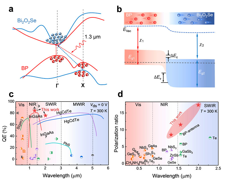 |
| Figure 1. Momentum-matching and band-alignment vdW BP/Bi2O2Se infrared photodetectors. a, Energy valley structure and transition of the BP/Bi2O2Se vdW heterojunction. b, Type II band alignment of the BP/Bi2O2Se vdW heterojunction. c, Comparison of QE of the BP/Bi2O2Se photodetector with 2D and bulk material photodetectors at zero bias. d, Comparison of polarization ratio under different wavelengths. (Image: SITP)
|
|
The photogenerated electrons and holes see no potential barriers and can be collected efficiently in type II BP/Bi2O2Se vdW heterojunction, shown in Figure 1b. Ultimately, the room temperature QE (84% at 1.3 µm and 76.5% at 2 µm) of the BP/Bi2O2Se device were achieved, which are higher than most reported 2D-based devices and even comparable to commercially state-of-the-art infrared photodetectors at zero bias as shown in Figure 1C. This high QE is caused by the high absorption coefficient, free-barrier band transport, and detection-free interfaces.
|
|
In addition, the polarization ratio of the BP/Bi2O2Se device at 2 µm is up to 17, as shown in Figure 1d. This is also superior to most photodetectors based on polarized materials or antenna-assisted structures in the short-wave infrared region.
|

