| Jan 18, 2023 |
Two technical breakthroughs make high-quality 2D materials possible
(Nanowerk News) Researchers have been looking to replace silicon in electronics with materials that provide a higher performance and lower power consumption while also having scalability. An international team is addressing that need by developing a promising process to develop high-quality 2D materials that could power next-generation electronics.
|
|
Sang-Hoon Bae, an assistant professor of mechanical engineering and materials science at the McKelvey School of Engineering at Washington University in St. Louis, is one of three researchers leading the multi-institutional work published in Nature ("Non-epitaxial single-crystal 2D material growth by geometrical confinement"), together with his doctoral student Justin S. Kim and postdoctoral research associate Yuan Meng.
|
|
The work, which includes two technical breakthroughs, is the first to report that their method to grow semiconductor materials, known as transition metal dichalcogenides (TMD), would make devices faster and use less power.
|
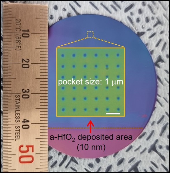 |
| Non-epitaxial single crystalline 2D materials at wafer-scale. (Image: Bae lab)
|
|
The team, co-led by Jeehwan Kim, an associate professor of mechanical engineering and of materials science and engineering at the Massachusetts Institute of Technology, and Jin-Hong Park, a professor of information and communication engineering and of electronic and electrical engineering at Sungkyunkwan University, had to overcome three extremely difficult challenges to create the new materials: securing single crystallinity at wafer-scale; preventing irregular thickness during growth at wafer-scale; and vertical heterostructures at wafer-scale.
|
|
Bae said 3D materials go through a process of roughening and smoothing to become an even-surfaced material. However, 2D materials don’t allow this process, resulting in an uneven surface that makes it difficult to have a large-scale, high-quality, uniform 2D material.
|
|
“We designed a geometric-confined structure that facilitates kinetic control of 2D materials so that all grand challenges in high-quality 2D material growth are resolved,” Bae said. “Thanks to the facilitated kinetic control, we only needed to grow self-defined seeding for a shorter growing time.”
|
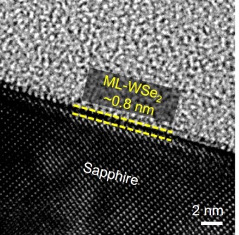 |
| Researchers report that their method to grow semiconductor materials, known as transition metal dichalcogenides (TMD), would make devices faster and use less power. (Image: Bae lab)
|
|
The team made another technical breakthrough by demonstrating single-domain heterojunction TMDs at the wafer scale, or a large scale, by layer-by-layer growth. To confine the growth of the nuclei, they used various substrates made from chemical compounds. These substrates formed a physical barrier that prevented lateral-epitaxy formation and forced vertical growth.
|
|
“We believe that our confined growth technique can bring all the great findings in physics of 2D materials to the level of commercialization by allowing the construction of single domain layer-by-layer heterojunctions at the wafer-scale,” Bae said.
|
|
Bae said other researchers are studying this material at very small sizes of tens to hundreds of micrometers.
|
|
“We scaled up because we can solve the issue by producing the high-quality material at large scale,” Bae said. “Our achievement will lay a strong foundation for 2D materials to fit into industrial settings.”
|

