| Jan 30, 2023 |
Topological acoustic waveguide to help reduce unwanted energy consumption in electronics(Nanowerk News) A team of researchers has developed a new acoustic waveguide based on the mathematical concept of topology, which will lead to reduced energy consumption in many everyday electronic devices. |
| Details of their innovation were published in the journal Physical Review Applied ("Imaging an Acoustic Topological Edge Mode on a Patterned Substrate with Microwave Impedance Microscopy"). |
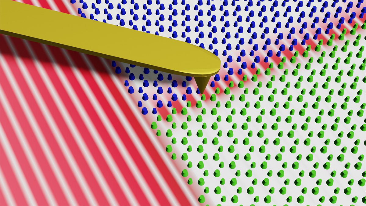 |
| A schematic of the topological surface acoustic waveguide. SAW is shown in red and white stripes that propagates into a metallic pillar pattern. The upper (blue) and lower (green) pillar patterns have a distinct topological acoustic property. As a result, a characteristic SAW mode appears along the interface between them. In the experiment, the SAW mode was directly visualized by scanning microwave impedance microscopy (brown). (Image: Yoichi Nii) |
| As their name implies, surface acoustic waves (SAW) are a type of acoustic wave where the vibration magnitude is focused on a material's surface. SAWs can be excited and detected on piezoelectric substrates, crystals with the ability to generate electricity when compressed or vibrated. Electrical components, known as SAW devices, make use of this and provide frequency filtering and sensing in common electronic devices such as mobile phones and touch sensors. But one drawback of SAW devices is that they consume a lot of energy, thus being a drain on battery life. |
| The team, which comprised Yoichi Nii and Yoshinori Onose from the Institute for Materials Research at Tohoku University, created a topological waveguide as a solution to this problem. |
| Waveguides are devices that carry or guide waves in a spatially confined area. Topological waveguides are a recent development that reduce energy loss and allow for manipulating waves in unique ways. The topological nature of the team's waveguide minimizes energy consumption and could drastically prolong the battery life of our phones and other electronics. |
| This waveguide also had the added benefit of being easy to create and compatible with current SAW device technology. "Implementing our waveguide involves simply fabricating nano-sized pillar patterns on the surface of the piezoelectric substrate," says Nii. |
| The waveguide could drive further breakthroughs in quantum technologies. "SAW based technologies have also attracted the attention of researchers exploring ways to push the boundaries of quantum computing," adds Nii. |
| Source: Tohoku University |

