| Feb 07, 2023 |
Microscopy images could lead to new ways to control excitons for quantum computing(Nanowerk News) Excitons are drawing attention as possible quantum bits (qubits) in tomorrow’s quantum computers and are central to optoelectronics and energy-harvesting processes. However, these charge-neutral quasiparticles, which exist in semiconductors and other materials, are notoriously difficult to confine and manipulate. |
| Now, for the first time, researchers have created and directly observed highly localized excitons confined in simple stacks of atomically thin materials. The work confirms theoretical predictions and opens new avenues for controlling excitons with custom-built materials. |
| “The idea that you can localize excitons on specific lattice sites by simply stacking these 2D materials is exciting because it has a variety of applications, from designer optoelectronic devices to materials for quantum information science,” said Archana Raja, co-lead of the project and a staff scientist at Lawrence Berkeley National Laboratory’s (Berkeley Lab) Molecular Foundry, whose group led the device fabrication and optical spectroscopy characterization. |
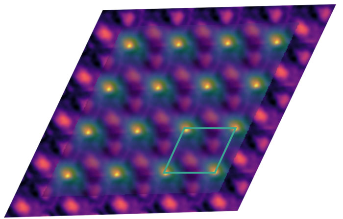 |
| This electron microscopy-derived composite image shows excitons in green. The moiré unit cell outlined in the lower right of the exciton map is about 8 nanometers in size. (Image: Sandhya Susarla and Peter Ercius, Berkeley Lab) |
| The team fabricated devices by stacking layers of tungsten disulfide (WS2) and tungsten diselenide (WSe2). A small mismatch in the spacing of atoms in the two materials gave rise to a moiré superlattice, a larger periodic pattern that arises from the overlap of two smaller patterns with similar but not identical spacing of elements. Using state-of-the-art electron microscopy tools, the researchers collected structural and spectroscopic data on the devices, combining information from hundreds of measurements to determine the probable locations of excitons. |
| “We used basically all the most advanced capabilities on our most advanced microscope to do this experiment,” said Peter Ercius, who led the imaging work at the Molecular Foundry’s National Center for Electron Microscopy. “We were pushing the boundaries of everything we can do, from making the sample to analyzing the sample to doing the theory.” |
| Theoretical calculations, led by Steven Louie, a faculty senior scientist at Berkeley Lab and distinguished professor of physics at UC Berkeley, revealed that large atomic reconstructions take place in the stacked materials, which modulate the electronic structure to form a periodic array of “traps” where excitons become localized. Discovery of this direct relationship between the structural changes and the localization of excitons overturns prior understanding of these systems and establishes a new approach to designing optoelectronic materials. |
| The team’s findings are described in a paper published in the journal Science ("Hyperspectral imaging of exciton confinement within a moiré unit cell with a subnanometer electron probe") with postdoctoral fellows Sandhya Susarla (now a professor at Arizona State University) and Mit H. Naik as co-lead authors. Next the team will explore approaches to tuning the moiré lattice on demand and making the phenomenon more robust to material disorder. |
| Source: By Alison Hatt, Lawrence Berkeley National Laboratory |

