| Apr 05, 2023 |
Hot probe tip contributes to making 'transformer' semiconductor particles
(Nanowerk News) How can we make wearable devices like Spiderman’s suit that are thin and soft yet also feature various electrical and optical functionalities? The answer lies in producing novel materials that go far beyond the performance of existing materials and developing technology that enables the precise control of the physical properties of such materials.
|
|
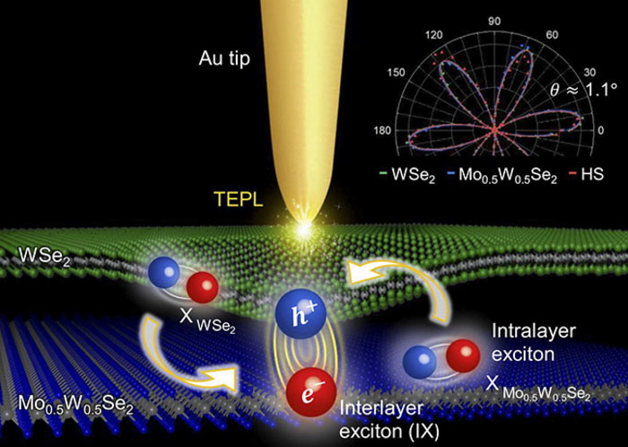
Separating transition metal dichalcogenide (TMD) into a single layer just like graphene makes it transform into a thin, two-dimensional (2D) film material that exhibits the characteristics of highly performing semiconductors. By stacking two disparate TMD layers, different combinations of TMD types and stacking methods can produce unique properties.
|
|
For this reason, 2D semiconductors based on heterostructures are attracting attention as an important next-generation material for the electronics industry throughout academia and industries around the world. However, it is still quite challenging to commercialize them due to the difficulty of controlling with precision the physical properties of their quasiparticles.
|
|
Professor Kyoung-Duck Park, Yeonjeong Koo, and Hyeongwoo Lee from the Department of Physics at POSTECH conducted a joint research with the team from ITMO University in Russia led by Professor Vasily Kravtsov to develop a multifunctional tip-enhanced spectroscopy that dynamically controls the quasiparticles of a 2D material in a small space. The team successfully controlled semiconductor particles such as interlayer excitons and interlayer trions that are formed at TMD heterobilayers by using the spectroscopy at about the 20nm level.
|
|
The research has been published in Light: Science & Applications ("Tunable interlayer excitons and switchable interlayer trions via dynamic near-field cavity").
|
 |
| Graphical abstract of the work. (Image: POSTECH)
|
|
Like excitons, interlayer excitons of TMD heterobilayers exhibit photoluminescence (PL), which is one of the properties of semiconductor materials. Interlayer excitons, which are electrically neutral quasiparticles, can be used in next-generation semiconductor devices with less heat as they are part light and part matter. They can also be used as a light source for quantum information technologies due to their longer coherence time than those of excitons. Still, there are several hurdles to overcome in their application. They have very low luminous efficiency at room temperature, and it is difficult to modulate their luminous energy.
|
|
The POSTECH team led by Professor Park, which had proposed technology for controlling excitons in nano-scale spaces in its previous research, successfully developed the multifunctional tip-enhanced spectroscopy that can be adjusted by gigapascal (GPa)-scale pressure and near-field intensity.
|
|
The spectroscopy can increase interlayer excitons’ luminous efficiency by about 9,000 times and dynamically modulate their luminous energy (the color of the light). In addition, the tip-based hot electron injection technology enabled the team to achieve the world’s first dynamic control of quasiparticle conversion between interlayer excitons and interlayer trions.
|
|
The most significant advantage of the research breakthrough is that it helps dynamically control the physical properties of the quasiparticles under the condition of room temperature and atmospheric pressure and analyze in real time the optical characteristics of semiconductor particles with the spatial resolution of about 20nm, which is far shorter than the wavelength of light.
|
|
Yeonjeong Koo, one of the two co-first authors of the research paper, explained, “The spectroscopy the team developed can be employed in identifying new physical properties of individual semiconductor particles such as interlayer excitons from the TMD heterobilayers. I am very much looking forward to the next physical discoveries.”
|
|
The research findings are expected to open up possibilities for various applications of 2D semiconductors based on heterostructures that are being extensively studied as a next-generation material. The fact that basic research in measuring instrument development contributed greatly to the outcome garnered even more attention in the field.
|
|
The technology is also expected to be used in developing high luminance, ultrathin wearable optoelectronic devices. The achievement is all the more meaningful in the current situation where the U.S., Japan, and China are vying for dominance in the semiconductor equipment market and putting up technology barriers.
|

