| Aug 01, 2023 |
Using sound waves to image nanostructures(Nanowerk News) The potential of an ultrafast form of transmission electron microscopy to measure sound waves in nanostructures has been demonstrated by three RIKEN physicists (Nano Letters, "Characterizing an optically induced sub-micrometer gigahertz acoustic wave in a silicon thin plate"). This could help realize a high-resolution imaging method that uses ultrahigh-frequency sound waves to image structures that are nanometers in size. |
| Ultrasound is routinely used in clinics and hospitals to image internal organs and babies in the womb. The sound waves used are usually a few millimeters in wavelength, and so they can image structures down to that level. |
| While such a resolution is fine for medical imaging, physicists would like to use sound waves to image structures in materials that are a few nanometers in size. |
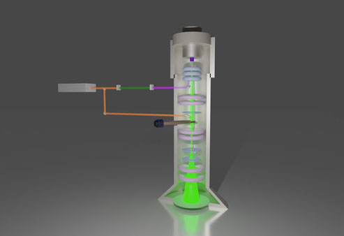 |
| A cutaway of the ultrafast transmission electron microscope (UTEM) that RIKEN researchers used to image ultrahigh-frequency sound waves in a thin silicon plate. The laser one the left provides two beams, one (upper beam) that interacts with the electron beam (green) of the microscope and the other (lower beam) illuminates the sample. (Image: RIKEN Center for Emergent Matter Science) |
| “If we can use sound waves that have wavelengths of about 100 nanometers or so, we can use them for inspecting materials, such as finding defects,” explains Asuka Nakamura of the RIKEN Center for Emergent Matter Science (CEMS). “But the sensitivity to small defects really depends on the wavelength.” |
| This requires generating and detecting sound waves that have much smaller wavelengths (and hence higher frequencies). Creating such high-frequency sound waves is relatively easy—ultrashort laser pulses have been used to generate them in metals and semiconductors for several decades. But detecting them is much more challenging since it requires developing detectors capable of achieving a resolution of nanometers in space and picoseconds in time. |
| Now, Nakamura, along with CEM colleagues Takahiro Shimojima and Kyoko Ishizaka, have demonstrated the potential of a special type of electron microscope for imaging such ultrahigh-frequency sound waves. |
| Specifically, they used an ultrafast transmission electron microscope (UTEM) to detect sound waves generated by a 200-nanometer hole in the center of an ultrathin silicon plate. A UTEM uses two laser beams with a slight delay between them (Fig. 1). One beam illuminates the sample, while the other generates an ultrashort pulse of electrons in the microscope. This setup enables very short timescales to be resolved. |
| When the trio simulated the waves theoretically and compared the simulations with experimentally obtained images, they found good agreement. |
| The quality of the images exceeded the team’s expectations, allowing them to perform Fourier-transform analysis—a commonly used mathematical analytic technique—on the images. “Before performing these experiments, we didn’t intend to characterize the sound waves,” says Nakamura. “But after taking the data, we noticed they were very beautiful, and we could apply Fourier transformation. That was surprising for me.” |
| The researchers now intend to investigate ultrafast structural and magnetic dynamics in solids induced by such nanometric sound waves using UTEM. |
| Source: RIKEN (Note: Content may be edited for style and length) |

