| Aug 01, 2023 |
A novel laser slicing technique for diamond semiconductors
(Nanowerk News) Silicon-based materials are currently the undisputed leaders in the field of semiconductors. Even so, scientists around the world are actively trying to find superior alternatives for next-generation electronics and high-power systems. Interestingly, diamonds are among the most promising materials for applications such as fast telecommunications and power conversion in electric vehicles and power plants.
|
|
Despite their attractive properties for the semiconductor industry, the applications of diamonds are limited due to the lack of techniques to slice them into thin wafers efficiently. As a result, diamond wafers must be synthesized one by one, making fabrication costs prohibitive for most industries.
|
|
Now, a research team from Japan, led by Professor Hirofumi Hidai from the Graduate School of Engineering at Chiba University, has found a solution to this problem. In a recent study in Diamond & Related Materials ("Laser slicing of a diamond at the {100} plane using an irradiation sequence that restricts crack propagation along the {111} plane"), they report a novel laser-based slicing technique that can be used to cleanly slice a diamond along the optimal crystallographic plane, thus producing smooth wafers. Their study is co-authored by master’s student Kosuke Sakamoto from the Graduate School of Science and Engineering at Chiba University and former Ph.D. student Daijiro Tokunaga, currently an Assistant Professor at Tokyo Institute of Technology.
|
 |
| Focusing the energy of a laser beam into a small volume of a diamond sample creates tiny ‘modified regions.’ If these modified regions are laid out in a precise grid-like pattern, the ensuing cracks make it easy to separate a {100} wafer from the diamond. (Image: Hirofumi Hidai, Chiba University)
|
|
The properties of most crystals, including diamonds, vary along different crystallographic planes—imaginary surfaces containing the atoms comprising the crystal. For instance, a diamond can be easily sliced along the {111} surface. However, slicing {100} is challenging because it also produces cracks along the {111} cleavage plane, increasing kerf loss.
|
|
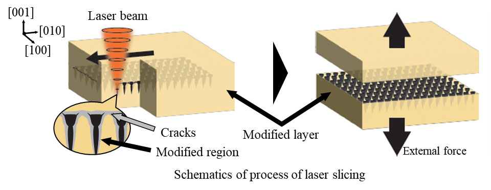
To prevent the propagation of these undesirable cracks, the researchers developed a diamond processing technique that focuses short laser pulses onto a narrow cone-like volume within the material. “Concentrated laser illumination transforms diamond into amorphous carbon, whose density is lower than that of diamond. Hence, regions modified by laser pulses undergo a reduction in density and crack formation,” explains Prof. Hidai.
|
|
By shining these laser pulses onto the transparent diamond sample in a square grid pattern, the researchers created a grid of small crack-prone regions inside the material. If the space between the modified regions in the grid and the number of laser pulses used per region are optimal, all modified regions connect to each other through small cracks that preferentially propagate along the {100} plane. Consequently, a smooth wafer with {100} surface can be easily separated from the rest of the block by simply pushing a sharp tungsten needle against the side of the sample.
|
|
Overall, the proposed technique is a pivotal step toward making diamonds a suitable semiconductor material for future technologies. In this regard, Prof. Hidai remarks: “Diamond slicing enables the production of high-quality wafers at low cost and is indispensable to fabricate diamond semiconductor devices. Therefore, this research brings us closer to realizing diamond semiconductors for various applications in our society, such as improving the power conversion ratio in electric vehicles and trains.”
|

