| Sep 21, 2023 |
All-optical generation of static electric field in a single metal-semiconductor nanoantenna
(Nanowerk News) Researchers have developed a new technique to generate static electric fields in nanoscale devices using only light. This discovery, published in Light: Science & Applications ("All-optical generation of static electric field in a single metal-semiconductor nanoantenna"), could enable faster computing speeds and more versatile nanophotonic devices.
|
|
At its core, computing relies on manipulating electric currents and fields. But as devices shrink to the nanometer scale, controlling these flows becomes increasingly difficult. Wires and transistors can't scale down infinitely, so scientists need new methods to induce electric forces within microscopic spaces.
|
|
Light offers a promising solution, as it can focus energy down to nanometer precision. In certain materials like silicon, shining light creates separated positive and negative charges - an electric field. The challenge lies in harnessing this photo-induced field inside nanodevices.
|
|
Now, researchers have accomplished this using hybrid metal-semiconductor nanoparticles. Their nanoantennas absorb light and generate powerful static fields at the junction between metal and semiconductor. Critically, the field arises from charge separation inherent to the nanoparticle rather than an external power source.
|
|
To make the nanoantennas, the researchers combined sophisticated lithography and ultrafast laser processing. This yielded gold nanodisks adhered to crystalline silicon nanocones via a thin chromium layer. The disk focused light to the metal-semiconductor interface, while silicon provided high charge mobility.
|
|
Beaming infrared laser pulses at the nanoantennas produced strong second harmonic light, indicating a strong electric field. Unlike most materials, silicon lacks inherent second order optical nonlinearity. But by breaking symmetry, the static field imparted second harmonic generation. This confirms the presence and strength of the optically induced field.
|
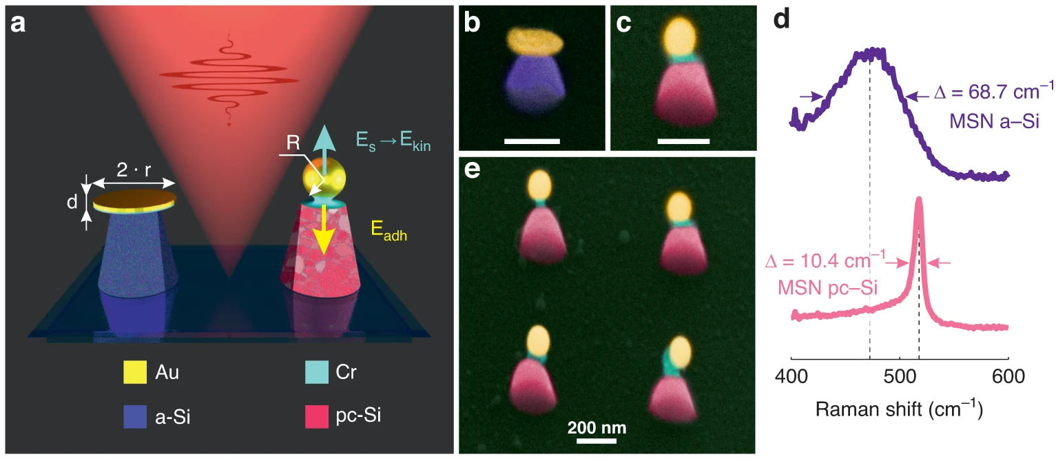 |
| a Schematic of the processes defining the gold component modification. SEM images b initial hybrid nanoparticle, c metal/high-refractive-index semiconductor nanostructure (scale bar of 200 nm). d Raman spectra of the hybrid nanoparticle before (violet curve) and after (pink curve) laser irradiation. Colors of the silicon component in the images indicate their crystalline state: violet means amorphous silicon, and pink crystalline silicon. e Array of the metal/high-refractive-index semiconductor nanostructure. (© Light: Science & Applications)
|
|
Remarkably, the second harmonic intensity increased much faster than the excitation power, following a fourth power dependence. Such nonlinear growth results from an “electric field induced second harmonic” (EFISH) effect in silicon, whereby the static field interacts with third order optical nonlinearities. The researchers tuned the nanoantenna geometry to maximize this EFISH contribution from the interface.
|
|
Time-resolved measurements revealed the field results from trapping photogenerated electrons at the interface. At higher light powers, the field reached strengths around 100 megavolts per meter. To interpret these nonlinear optical effects, the team modeled nanoscale carrier dynamics using the drift-diffusion approximation. This quantified how light absorption, charge separation, and surface trapping collaborate to build the static field.
|
|
Silicon’s electronic properties proved essential for this all-optical field generation. Its band structure allows efficient photogeneration of electrons even with infrared light. Meanwhile, high mobility permits transport to the metal-semiconductor junction before recombination. There, band bending localizes the electrons and yields a strong field.
|
|
Besides confirming this mechanistic picture, the simulations explored how nanoantenna geometries influence the EFISH response. Closer metal-semiconductor contact enhanced light absorption at the junction, which strengthened the static field and nonlinear growth of second harmonic generation. This nonlinear optical effect directly reported on the interfacial field.
|
|
By leveraging silicon’s advantages, the researchers achieved all-optical electric field generation in a nanoscale volume. This photoinduced field reaches strengths comparable to those applied externally in microelectronic devices. Harnessing the field at the nanoscale could enable faster operation and greater energy efficiency.
|
|
The study demonstrates a versatile new platform for optoelectronic devices and on-chip signal processing. Within each nanoantenna, light controls electricity. Arranging many such pixels on a chip would allow all-optical manipulation of nanocircuitry. Though still early-stage, the prospects include replacing electronics with faster optical computing.
|
|
More immediately, the nanoantennas’ electric field sensitivity and ultrafast response can improve sensing and imaging. Characterizing how the EFISH response depends on wavelength and polarization will enhance nanoscale field visualization. By tailoring silicon’s properties through dopants and defects, researchers can also optimize the photoinduced field strength.
|
|
This breakthrough results from engineering both nanophotonic and semiconductor physics within a single nanostructure. While more development is needed, the study opens the door to nanodevices that integrate optics and electronics in new ways. Leveraging silicon provides a path to incorporate these photo-active nanoantennas into existing nanofabrication workflows. With further progress, this new optoelectronic functionality could find widespread use in telecommunications, computing, and related fields.
|

