| Dec 01, 2023 |
2D material reshapes 3D electronics for AI hardware
(Nanowerk News) Multifunctional computer chips have evolved to do more with integrated sensors, processors, memory and other specialized components. However, as chips have expanded, the time required to move information between functional components has also grown.
|
|
“Think of it like building a house,” said Sang-Hoon Bae, an assistant professor of mechanical engineering and materials science at the McKelvey School of Engineering at Washington University in St. Louis. “You build out laterally and up vertically to get more function, more room to do more specialized activities, but then you have to spend more time moving or communicating between rooms.”
|
|
To address this challenge, Bae and a team of international collaborators, including researchers from the Massachusetts Institute of Technology, Yonsei University, Inha University, Georgia Institute of Technology and the University of Notre Dame, demonstrated monolithic 3D integration of layered 2D material into novel processing hardware for artificial intelligence (AI) computing. They envision that their new approach will not only provide a material-level solution for fully integrating many functions into a single, small electronic chip, but also pave the way for advanced AI computing.
|
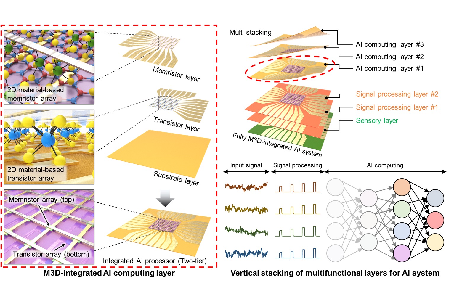 |
| Schematic illustration of an edge computing system based on monolithic 3D-integrated, 2D material-based electronics. The system stacks different functional layers, including AI computing layers, signal-processing layers and a sensory layer, and integrates them into an AI processor. (Image: Sang-Hoon Bae)
|
|
Their work was published in Nature Materials ("Monolithic 3D integration of 2D materials-based electronics towards ultimate edge computing solution"), where it was selected as a front cover article.
|
|
The team’s monolithic 3D-integrated chip offers advantages over existing laterally integrated computer chips. The device contains six atomically thin 2D layers, each with its own function, and achieves significantly reduced processing time, power consumption, latency and footprint. This is accomplished through tightly packing the processing layers to ensure dense interlayer connectivity. As a result, the hardware offers unprecedented efficiency and performance in AI computing tasks.
|
|
This discovery offers a novel solution to integrate electronics and also opens the door to a new era of multifunctional computing hardware. With ultimate parallelism at its core, this technology could dramatically expand the capabilities of AI systems, enabling them to handle complex tasks with lightning speed and exceptional accuracy, Bae said.
|
|
“Monolithic 3D integration has the potential to reshape the entire electronics and computing industry by enabling the development of more compact, powerful and energy-efficient devices,” Bae said. “Atomically thin 2D materials are ideal for this, and my collaborators and I will continue improving this material until we can ultimately integrate all functional layers on a single chip.”
|
|
Bae said these devices also are more flexible and functional, making them suitable for more applications.
|
|
“From autonomous vehicles to medical diagnostics and data centers, the applications of this monolithic 3D integration technology are potentially boundless,” he said. “For example, in-sensor computing combines sensor and computer functions in one device, instead of a sensor obtaining information then transferring the data to a computer. That lets us obtain a signal and directly compute data resulting in faster processing, less energy consumption and enhanced security because data isn’t being transferred.”
|

