| Feb 13, 2024 |
Nanoparticle 3D-printing technology applicable to inorganic materials(Nanowerk News) A collaborative team of researchers from Pohang University of Science and Technology (POSTECH), led by Professor Jae Sung Son from the Department of Chemical Engineering, and Korea Institute of Science and Technology, under the leadership of Dr. Jin Young Kim, employed linker ions to pioneer a three-dimensional microprinting technology applicable to inorganic substances and other various materials. |
| Their work has been published in Nature Communications ("3D microprinting of inorganic porous materials by chemical linking-induced solidification of nanocrystals"). |
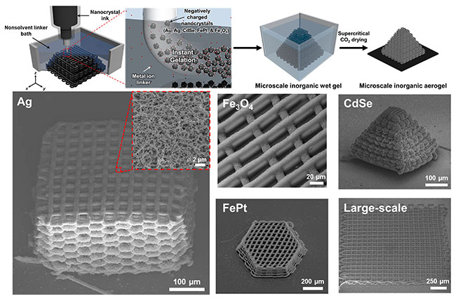 |
| Above: Schematic representation of nanoparticle 3D printing. Below: Produced microstructures. (Image: POSTECH) |
| Three-dimensional microprinting is a cutting-edge process used in electronic communications, biotechnology, healthcare and many other areas, and represents the next generation of manufacturing small components and sensors, aligning with the recent trends of device miniaturization and lightweight design. However, traditional 3D microprinting has faced challenges in maintaining structures, particularly with inorganic materials such as metals, where controlling nano-sized particles proved difficult. |
| To address this challenge, the research team adopted transition metal cations as linker ions in their recent study. Linker ions selectively react on the surfaces of nanoparticles and promote bonding and interactions among particles, inducing their rapid solidification. |
| The team employed 3D microprinting technology to deposit inorganic nanoparticles into a linker ion bath. The linker ions caused the formation of interconnected networks among the dispersed inorganic nanoparticles, allowing the particles to rapidly solidify and maintain the overall structure. |
| Moreover, the team managed to craft inorganic porous structures with dimensions below 10 μm by fine-tuning the interactions between particles, surpassing the limitations of conventional microprinting and achieving inorganic material printing without the need for specialized equipment. |
| This research showcases the versatility of their technology, demonstrating its applicability to wide range of functional inorganic materials, including metals, semiconductors, magnets, and oxides. Significantly, their method holds promise for replacing the conventional high-cost and time-consuming processes in manufacturing components for electronic devices, such as micro-electro-mechanical systems (MEMS). |
| POSTECH Professor Jae Sung Son remarks, “Our research introduces a new pathway for effortlessly creating three-dimensional structures with improved solution processing technology for nano-printing. It is poised to play a crucial role in further research on nano-material-based devices.” Dr. Jin Young Kim from KIST also expressed hopes, saying “We look forward to the commercialization of various materials and components made possible by the improved quality of large-area structures and enhanced production speed brought about by our process technology.” |
| Source: Pohang University of Science and Technology (Note: Content may be edited for style and length) |

