| Mar 05, 2024 |
A novel method for studying brain-like circuitry in nanomaterials
(Nanowerk News) Artificial intelligence (AI) has the potential to transform technologies as diverse as solar panels, in-body medical sensors and self-driving vehicles. But these applications are already pushing today’s computers to their limits when it comes to speed, memory size and energy use.
|
|
Fortunately, scientists in the fields of AI, computing and nanoscience are working to overcome these challenges. And they are using their brains as their models.
|
|
That is because the circuits, or neurons, in the human brain have a key advantage over today’s computer circuits: they can store information and process it in the same place. This makes them exceptionally fast and energy efficient. That is why scientists are now exploring how to use nanomaterials to construct circuits that work like our neurons. To do so successfully, however, scientists must understand precisely what is happening within these nanomaterial circuits at the atomic level.
|
|
Recently, a team of researchers including scientists from the U.S. Department of Energy’s (DOE) Argonne National Laboratory pioneered a novel way of evaluating exactly that. Specifically, they used the Advanced Photon Source (APS), a DOE Office of Science user facility, to examine the changes that occur in the structure of a specific nanomaterial as it changes from conducting an electrical current to not. This mimics the switching between “on” and “off” states in a neural circuit.
|
|
In these materials, the conducting state, or phase, is controlled by imperfections in the material (or “point defects”) at the atomic level. By putting a strain on the nanomaterial, researchers can alter the concentration and change the position of these defects. This changes the pathway of electron flow. However, these defects are constantly moving, which changes the material’s conducting and non-conducting regions. Until now, this motion has been extremely difficult to study.
|
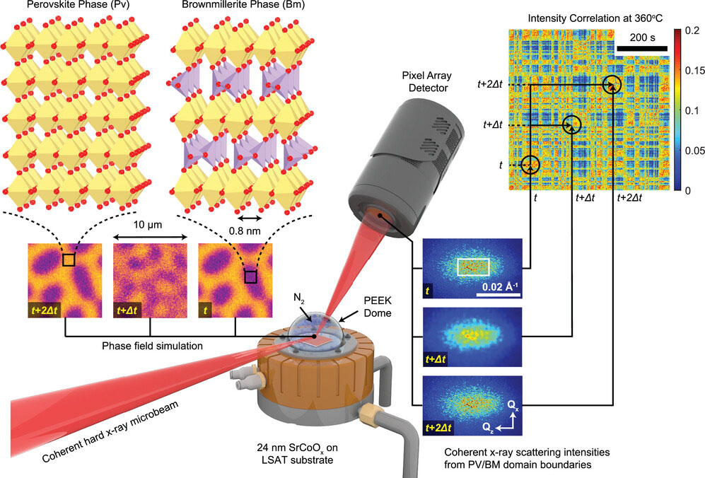 |
| This diagram illustrates how the researchers arrayed the APS to examine how the structure of a specific material, SrCoOx, changes when it is conducting an electrical current versus when it is not. (Image: Advanced Materials) (click on image to enlarge)
|
|
The researchers describe the experimental details and their findings in Advanced Materials ("Intermittent Defect Fluctuations in Oxide Heterostructures").
|
|
“There has been a lot of research about the occurrence and nature of defects in nanomaterials,” explained Dillon Fong, a materials scientist at Argonne. “But we knew very little about the dynamics of these defects when a material changes phase. We wanted to show that you can use X-rays to examine transitions between conducting and non-conducting phases in nanomaterials under conditions similar to those under which these materials will be used.” The team demonstrated how the APS can help make this possible.
|
|
For the experiment, the researchers chose a material, SrCoOx, that easily switches between the conducting and non-conducting, insulating, phases. To see the fluctuation between the conducting phase and the insulating phase at the nanoscale, they used a technique called X-ray photon correlation spectroscopy (XPCS). This is enabled by the highly coherent X-ray beams from the APS. XPCS can directly measure how fast the material fluctuates between different phases at the atomic scale, even when these fluctuations are barely detectable.
|
|
“The XPCS measurement would not be possible without the coherent X-ray beam from the APS,” said Qingteng Zhang, an assistant physicist at the APS who led the X-ray measurements. “In addition, it is important that we take the measurement under the same conditions that the material will operate under. This allows us to learn how the material will behave while performing its intended function. However, such environmental control usually requires sealing the sample in a chamber or a dome. This is where the highly penetrating X-ray beam from the APS is extremely helpful. Because while the chamber window or the dome shell is opaque to visible light, we can make either one completely transparent to the X-rays.”
|
|
The APS upgrade — now underway — will increase the brightness of the APS X-rays by up to 500 times upon its completion in 2024. This will significantly increase the speed of measurement as well as the quality of coherent X-ray techniques, including XPCS. This could create unprecedented scientific opportunities for researchers around the world.
|
|
That is an exciting prospect for Panchapakesan Ganesh, a researcher at DOE’s Oak Ridge National Laboratory (ORNL). He led the theoretical work in the study along with his team members Vitalii Starchenko, ORNL, and Guoxiang Hu, now an assistant professor at Georgia Tech.
|
|
“High-quality data from experiments like these are critical to our ability to develop theories and build models that can capture what happens in nanoelectronic materials when they go from conducting to non-conducting phases,” Ganesh said. “For example, we need to learn how energy dissipates in these systems if we are going to develop nanodevices that approach the energy efficiency of our brains. No single computational approach can solve this type of problem on its own. We need the best inputs from both the experimental and computational science sides to advance this nanoscale understanding. Our integrated approach is a perfect example of that, and we think it will spur more research in this exciting new field.”
|


