| Posted: Jul 16, 2017 |
A high-resolution transfer printing method for graphene inks(Nanowerk News) Researchers have demonstrated here a transfer printing method based on a hydrophobic mold suitable for high-resolution patterning of graphene inks. |
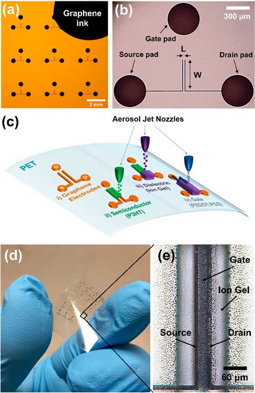
| As the team reports in ACS Nano ("High-Resolution Transfer Printing of Graphene Lines for Fully Printed, Flexible Electronics"), the robust thermal stability of the mold (∼250°C) allows broad process compatibility, enabling printing of conductive, flexible, sub-5 µm graphene patterns. |
 |
| CAPTION |
| Over the past few years, high-resolution printing of electronically functional inks on plastic or paper substrates is a compelling manufacturing platform for large-area, low-cost, flexible electronic systems with applications in sensors, displays, energy devices, smart packaging, and radio frequency identification. |
| The demonstrated printing resolution for pristine graphene inks has to-date been limited to 30 µm, primarily due to lateral spreading of the functional inks which results in low aspect ratio features with suboptimal conductance. |
| The development of high-performance flexible electronic devices however requires a reliable route to printed graphene patterns with line width and spacing of just a few microns. |
| In addition, line edge roughness decreases print consistency and yield for high-resolution, closely spaced features such as transistor electrodes. |
| In their present work, the researchers demonstrated excellent conductivity and flexibility of the graphene electrodes and utilized them for fully printed electrolyte-gated transistors tolerant to tensile strains of 1% over 1000 bending cycles. |
| By leveraging the high-fidelity printing process, capable of achieving line edge roughness below 25 nm, the transistor channel length could be scaled to ∼1 µm, offering a compelling advantage for progress in the scalable fabrication of nanoelectronic devices. |
| "This promising platform for transfer printing offers significant potential for expanding the design space to integrate functional inks with precise, high-resolution patterning methods, ultimately advancing the development of high-performance, flexible, printed electronic systems," the authors cocnlude their work. |
 By
Michael
Berger
– Michael is author of four books by the Royal Society of Chemistry:
Nano-Society: Pushing the Boundaries of Technology (2009),
Nanotechnology: The Future is Tiny (2016),
Nanoengineering: The Skills and Tools Making Technology Invisible (2019), and
Waste not! How Nanotechnologies Can Increase Efficiencies Throughout Society (2025)
Copyright ©
Nanowerk LLC
By
Michael
Berger
– Michael is author of four books by the Royal Society of Chemistry:
Nano-Society: Pushing the Boundaries of Technology (2009),
Nanotechnology: The Future is Tiny (2016),
Nanoengineering: The Skills and Tools Making Technology Invisible (2019), and
Waste not! How Nanotechnologies Can Increase Efficiencies Throughout Society (2025)
Copyright ©
Nanowerk LLC
|
|
Subscribe to a free copy of one of our daily Nanowerk Newsletter Email Digests with a compilation of all of the day's news. |