| Dec 05, 2011 |
Separating a single-layer of quantum dots with insulation increases efficiency |
| (Nanowerk News) Efficiency in quantum dot (QD) devices is reduced by energy flowing between the dots instead of escaping as light perpendicular to the QD layer. Now, using an atomic layer deposition process, researchers at Harvard University have developed a way to separate individual QDs within a single layer with an aluminum oxide (Al2O3) insulating layer. Edward Likovich, lead author of the paper, says the best metaphor is a carton of eggs, with the CdSe/ZnS QDs representing the eggs and the Al2O3 layer representing the cardboard spacers in between them. |
| "The process provides a mechanical and energetic barrier between adjacent quantum dots, so the current tends to flow perpendicularly as opposed to being dissipated among dots in the layer," Likovich says. "Also, because we have this mechanical barrier between the dots, we can do post-processing to remove the ligands while holding the dots in place, preventing agglomeration." |
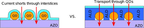 |
| In an early design (left), the path of least resistance was between the quantum dots, so the current bypassed the dots and produced no light. Using the atomic layer deposition (ALD) technique (right), researchers were able to funnel current directly through the dots, creating a fully functional, single-layered QD-LED. (Image: Edward Likovich) |
| Quantum dots are being studied for many potential applications. The luminescent properties of QDs are currently being used to increase the efficiency of LEDs, and they may soon be used in televisions and other displays. Likovich says QDs are also being investigated as light collectors instead of light emitters, for use as solar collectors to increase the efficiency of solar cells. |
| As reported in Advanced Materials ("High-Current-Density Monolayer CdSe/ZnS Quantum Dot Light-Emitting Devices with Oxide Electrodes"), Likovich and his coworkers started with a glass slide coated with Al-doped ZnO (AZO) as the bottom electrode of an LED. They then transferred a single layer of CdSe/ZnS core/shell QDs coated with hydrophobic octadecylamine ligands to the substrate. The Al2O3 insulating layer was produced at 150°C by alternating pulses of an organometallic compound containing Al with pulses of water, which served as the source of oxygen. "Because the dots are coated in ligands that are hydrophobic, this atomic layer deposition process tends to fill in the areas between the dots rather than coating the dots," Likovich says. A top AZO electrode was added to complete the device. |
| When a voltage was applied to the top and bottom electrodes, the current flowed directly through the QDs, causing luminescence by electron-hole recombination. In contrast, in a similar device having only Al2O3 tunnel barriers instead of an insulating layer, the current flowed between the QDs, preventing recombination and luminescence. |
| Future research plans are to investigate post-processing chemical treatments to either remove or swap ligands. Recent studies suggest that ligands may cause charging of the surfaces of QDs, reducing their efficiency, Likovich says. |
| Source: MRS |

