| Posted: March 6, 2008 |
IBM scientists 'quiet' unruly electrons in atomic layers of graphite |
|
(Nanowerk News) IBM researchers today announced a discovery that combats one of the industry's most perplexing problems in using graphite -- the same material found inside pencils -- as a material for building nanoelectonic circuits vastly smaller than those found in today's silicon based computer chips.
|
|
For the first time anywhere, IBM scientists have found a way to suppress unwanted interference of electrical signals created when shrinking graphene, a two-dimensional, single-atomic layer thick form of graphite, to dimensions just a few atoms long.
|
|
Scientists around the world are exploring the use of graphene as a much smaller replacement for today's silicon transistors. Graphene is a two-dimensional honeycomb lattice of carbon atoms, similar to atomic-scale chicken-wire, which has attracted strong scientific and technological interest because it exhibits promising electrical properties and could be used in transistors and circuits at scales vastly smaller than components inside of today's tiniest computer chips.
|
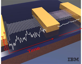 |
| The image on the left shows a single layer, or sheet of carbon molecules known as Graphene. The noise that occurs from electrical signals bouncing around in the material as a current is passed through it is greater as the device is made smaller and smaller, impeding the performance for nanoscale electronics. In the image on the right, the IBM scientists demonstrated for the first time that adding a second sheet of Graphene reduces the noise significantly, giving promise to this material for potential use in future nanoelectronics.
|
|
One problem in using these nano-devices is the inverse relationship between the size of the device and the amount of uncontrolled electrical noise that is generated: as they are made smaller and smaller, the noise -- electrical charges that bounce around the material causing all sorts of interference that impede their usefulness -- grows larger and larger. This trend is known as Hooge's rule, and occurs in traditional silicon based devices as well as in graphene nano-ribbons and carbon nanotube based devices.
|
|
"The effect of noise from Hooge's rule is exaggerated at the nanoscale because the dimensions are approaching the nearly smallest limits, down to only a handful of atoms, and the noise that is created can overwhelm the electrical signal that needs to be achieved to be useful," said IBM Researcher Dr. Phaedon Avouris, who leads IBM's exploration into carbon nanotubes and graphene. "To quote the famous physicist Rolf Landauer, at the nanoscale 'the noise is your signal'; in other words, you cannot produce any useful electronic device at the nanoscale if the noise is comparable to the signal you are trying to switch on and off."
|
|
Now, IBM scientists have found that the noise in graphene-based semiconductor devices can, in fact, be suppressed and report the results today in the journal Nano Letters ("Strong Suppression of Electrical Noise in Bilayer Graphene Nanodevices").
|
|
In their experiments, the IBM Researchers first used a single layer, or sheet, of graphene to build a transistor and noted that the device does in fact follow Hooge's Rule: as they are made smaller and smaller, there is an increase in the noise that is created.
|
|
Two Layers Are Better Than One
|
|
However, when the IBM Researchers built the same device with two sheets of graphene instead of one -- one stacked on top of the other -- they noted that the noise is suppressed, and is weak enough that these so-called bilayer graphene ribbons could prove useful for building future semiconductor devices for use in sensors, communications devices, computing systems and more. The noise is inhibited because of the strong electronic coupling between the two graphene layers that counteracts the influence of the noise sources: the system acts as a noise insulator.
|
|
While further detailed analysis and studies are required to better understand these phenomena, the findings provide exciting opportunities for graphene bilayers in a variety of applications.
|

