| Feb 06, 2013 |
High performance transistors on polymer superior to silicon
|
|
(Nanowerk News) Tatsuro Maeda and Taro Itatani, New Materials and Devices Integration Group, the Nanoelectronics Research Institute of the National Institute of Advanced Industrial Science and Technology (AIST), have developed technologies for transferring compound semiconductors using a polymer as a bonding adhesive and for fabricating high-performance transistors on a polymer, in collaboration with Sumitomo Chemical Co., Ltd.
|
|
Based on the respective strengths of AIST's substrate-bonding and device-fabrication technologies and Sumitomo Chemical's compound crystal growth technology, the researchers have developed (1) an adhesive polyimide with excellent heat resistance; (2) a transfer technology for a high-quality indium gallium arsenide (InGaAs) layer on a silicon substrate using the adhesive polyimide; and (3) a technology for fabricating transistors at temperatures below 400°C whose performance surpasses that of silicon transistors. These are important technical steps toward integrating post-silicon material devices and silicon large-scale integrated circuits (Si-LSI).
|
|
The developed technologies will make it possible to develop high-performance, multifunction devices integrating post-silicon materials and Si-LSI and to realize denser three-dimensional integration of electronic and photonic devices. Consequently, power consumption reduction, increase in speed, and downsizing of computers can be expected.
|
|
Details of the technologies were presented at the 2012 International Conference on Solid State Devices and Materials (SSDM 2012) held in Kyoto from September 25 to 27, 2012.
|
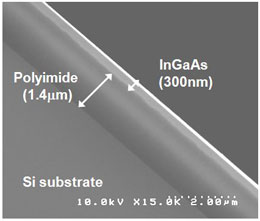 |
| Cross-sectional SEM image of InGaAs layer on polyimide.
|
|
Social Background of Research
|
|
Compound semiconductors and germanium, whose carrier mobility is superior to that of silicon, are called post-silicon materials, and research into them is proceeding in various countries as next-generation channel materials. Because such post-silicon materials do not replace all Si-LSI functions, post-silicon devices with the required performance must be mounted and perform a special function at the necessary places on Si-LSIs. Thus, a new technology known as back-end integration is needed, in which high-quality post-silicon materials are transferred onto a fabricated Si-LSI, and then devices are fabricated and interconnected with underlying Si-based circuits. Because many post-silicon materials have excellent optical properties that silicon does not, the back-end integration technology is expected as a platform technology for the functional integration of Si-LSIs and photonic devices.
|
|
History of Research
|
|
AIST and Sumitomo Chemical have been conducting joint research since 2008 on a hybrid semiconductor technology, which aims to integrate electronic and photonic devices. Their research has endeavored to integrate high-performance semiconductors on a silicon substrate with compound semiconductors or germanium that have a variety of functions as photonic materials. In the present research, they have developed a bonding technology for high-performance semiconductor crystal and a low-temperature device-fabrication technology toward functional integration of post-silicon and silicon devices utilizing AIST's world-class technologies for substrate bonding and device fabrication and Sumitomo Chemical's commercial-level compound semiconductor epitaxial growth technology.
|
|
Details of Research
|
|
Back-end integration is the formation of functional devices, not during the fabrication process of Si transistors on a silicon wafer (the front-end process), but rather during the process for wiring between elements such as transistors (the back-end process). And new functions are added to the existing Si-LSIs by connecting the formed devices with underling Si-LSIs (Fig. 1). It has been reported that the temperature when fabricating devices with post-silicon materials is 400°C or lower, compared to more than 1000°C with silicon materials (AIST press release on June 12, 2011). Therefore, post-silicon materials are suited for fabrication of devices in back-end processes, where low-temperature processes of at most 500°C are required. Moreover, lower process temperatures enable us to introduce inexpensive functional polymeric materials to semiconductor device processes, where inorganic materials have been the most common to date. In this research, the transfer technology of extremely thin (less than 300 nm) post-silicon materials onto silicon using polyimide and the fabrication technology of high performance transistors at 400°C or lower using a semiconductor layer directly attached to the polymer have been developed. For the first time, polyimide was directly attached to an extremely thin semiconductor active layer, transistors with performance superior to that of silicon transistors were fabricated, and their operation was confirmed.
|
 |
| Figure 1: Back-end integration technology for post-silicon materials.
|
|
The developed fabrication method of high-performance transistors as a back-end integration method is illustrated in Fig. 2. First, a high-quality InGaAs layer (300 nm), as a post-silicon material, is epitaxially grown on a lattice-matched indium phosphide (InP) substrate (Fig. 2 (a)). Next, the silicon substrate, coated with polyimide as an adhesive by spin-coating, is flipped over and attached to the epitaxially grown substrate (Fig. 2 (b)). A new polyimide with high heat resistance of greater than 450°C and high adhesiveness was developed to bond the post-silicon material (Fig. 3). Next, the InP substrate is selectively removed and a thin-film InGaAs crystal layer is obtained on the silicon substrate (Fig. 2 (c)). Finally, high performance transistors are fabricated at a process temperature of under 400°C using the obtained InGaAs layer on the polyimide/silicon substrate (Fig. 2 (d)). Polyimide has the major advantages of being very inexpensive and easy to handle as an adhesive material. The durability of the developed polyimide during the layer transfer and transistor-fabrication processes has been verified.
|
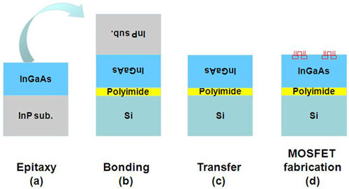 |
| Figure 2: Fabrication method of transistors on polyimide.
|
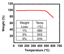 |
| Figure 3: Property of polyimide used for adhesion. There is almost no loss of mass up to about 500°C.
|
|
Figure 4 shows the performance of an InGaAs n-type MOSFET with 50 µm gate length on the polyimide. The drain current - gate voltage characteristics indicate excellent switching characteristics with an on/off ratio of larger than double digits, and the drain current - drain voltage characteristics with clear linear and saturated regions confirm good transistor operation (Fig. 4, left and center). The right side of Fig. 4 shows the mobility characteristics of InGaAs on InP substrate prior to transfer and on polyimide. Even on polyimide, the mobility of InGaAs is higher than 1000 cm2/Vs at most, or nearly twice as high as that of silicon. Compared to the mobility of InGaAs on InP substrate, although a slight decrease is observed in the low-carrier-density region, the mobility of InGaAs on polyimide is in conformity in the high-carrier-density region. During transistor fabrication, the polyimide is subjected to various heat cycles and chemical treatments, so at first there was concern that the polyimide would be a source of contamination during the process, which leads to degradation of transistor properties. The results, however, indicate that the polyimide behaves well enough as a permanent material for post-silicon semiconductors. It was also found that the transfer process has no adverse impact on the semiconductor properties, since no major degradation was found in device characteristics when compared before and after transfer. Since the transfer technology using polyimide and the low-temperature transistor-fabrication technology with post-silicon materials have been verified in this research, the integration of Si-LSIs with post-silicon devices as well as the introduction of polymer materials in a back-end process can be easily achieved. It is expected that high-performance, multifunction devices will be realized taking advantage of the diversity of polyimide and post-silicon materials.
|
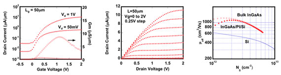 |
| Figure 4: Performance of InGaAs n-type MOSFET on polyimide. Good switching characteristics with an on/off ratio of larger than double digits (left). Clear linear and saturated regions are observed (center). Mobility of InGaAs on polyimide is about twice as large as that of silicon (right).
|
|
Future Plans
|
|
In the future, post-silicon materials, including InGaAs, will be used not only in high performance CMOS but also in various fields like one-chip electronic and photonic devices. Higher performance, more diverse functionality, and larger-scale integration that are impossible with past technology are anticipated because of the developed transfer technology for post-silicon material layers. Furthermore, since photosensitivity can be added to the polyimide whose process durability was verified, the polyimide would be formed in any location or be secondarily processed for wiring, and thus it would be very effective in high-level three-dimensional layered integration. To further enhance the back-end integration technology of post-silicon materials, the researchers aim to develop technology that supplies the necessary size of post-silicon materials to the necessary location to fabricate high-performance, multifunction devices.
|

