| Feb 19, 2013 |
Researchers fabricate a transistor with a channel length of 3 nanometers
|
|
(Nanowerk News) Shinji Migita and others, Collaborative Research Team Green Nanoelectronics Center, the Nanoelectronics Research Institute of the National Institute of Advanced Industrial Science and Technology (AIST), have confirmed the operation of an ultra-miniaturized transistor with a channel length of 3 nm.
|
|
The developed transistor was fabricated employing a V-shaped groove created by anisotropic dissolution of silicon crystal in an alkaline solution. By controlling the conditions of dissolution, a groove with a sharp tip measures 3 nm was prepared and the groove tip was used as the channel. Junctions were formed by a new technique whereby impurities are uniformly distributed on the entire silicon crystal. In terms of electrical characteristics, the current-regulating performance was maximized when the thickness of the channel (whose length is 3 nm) was thinned down to 1 nm. The velocity of electrons in the transistor was also investigated; it was verified that scattering effects are repressed inside the 3 nm-long channel, resulting in a quasi-ballistic flow of electrons. This suggests that an electric current can flow without energy loss. Consequently, reduction in power consumption of integrated circuits is expected.
|
|
Details of this technology were presented at the 2012 International Electron Devices Meeting (IEDM 2012) held in San Francisco, USA, from December 10 to 12, 2012.
|
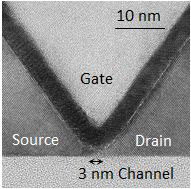 |
| Electron microscope image of transistor prototype with a channel length of 3 nm.
|
|
Social Background of Research
|
|
In recent years, the increase in power consumption associated with the spread of mobile information terminals and the progress in IT devices has become a concern. Social demand for reduction of the power consumed by electronic information devices is increasing. Large scale integrated circuits (LSIs), the core of electronic information devices, contain over 100 million transistors that perform high-speed operations. In order to reduce the power consumption of information devices, it is necessary to develop technology that will decrease the energy consumed by these millions of transistors.
|
|
R&D has been conducted globally to reduce the energy consumed by transistors from a variety of perspectives such as materials, structure, and operational principles. In structure, an important design strategy is to miniaturize transistors. Today, some LSIs on the market are made up of transistors measuring approximately 20 nm. At an R&D level, the performance verification on transistors measuring smaller than 10 nm is attracting attention.
|
|
History of Research
|
|
GNC was established in April 2010 to carry out a project adopted by FIRST operated by the Cabinet Office and the Japan Society for the Promotion of Science. GNC is comprised of AIST researchers and corporate researchers from five companies (Fujitsu Laboratories Ltd., Toshiba Corporation, Hitachi, Ltd., Renesas Electronics Corporation, and ULVAC, Inc.). GNC has been conducting research and development of transistors since FY 2011 aiming at reducing the power consumption of conventional LSIs to about 1/10 to 1/100 of their current levels.
|
|
This research was supported by “Development of Core Technologies for Green Nanoelectronics” project (Core Researcher: Naoki Yokoyama) of FIRST.
|
|
Details of Research
|
|
The developed technology was achieved employing the existing fabrication methods of semiconductors and incorporating a nanometer-scale structure-control technology and a new junction technology. Figure 1 shows the prototype procedures. A transistor was manufactured using an SOI substrate where a silicon single crystal is pasted onto an insulator film. First, an alkaline solution was used to dissolve a limited region of the single crystal to form a V-shaped groove. The dissolving speed varies significantly depending on the silicon crystal surface and, because of this property, only certain crystal surfaces remain, and a V-shaped groove is formed. By controlling the temperature and duration of dissolution, the tip of the groove can be made sharp, with a curvature radius of 3 nm. This part becomes the transistor channel. The channel thickness can be easily controlled by precisely adjusting the depth of the V-shaped groove. After the V-shaped groove is formed, gate insulator and gate electrode layers are deposited and pattern processing is carried out, creating a gate electrode. Then ions are implanted into what will become the source and the drain parts. Finally, high-temperature annealing was used to promote the diffusion of impurities so that they are distributed uniformly with a high concentration over the entire silicon crystal. In the conventional manufacturing method of transistors, the diffusion of impurities was inhibited to create a concentration gradient so PN junctions would be formed. However, when the transistor is miniaturized to less than 10 nm, the formation of PN junctions is difficult. To address this issue, a new junction technology was adopted whereby the transistor is operated only by the energy barrier created by the electric field of the gate electrode and no PN junction is used. Figure 2 shows an electron microscope image of the cross-sectional structure of the prototype transistor.
|
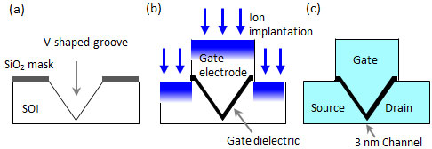 |
| Figure 1: Prototype procedures for the developed transistor. (a) An SOI substrate is dissolved to form a V-shaped groove using an alkaline solution. (b) Gate insulator and electrode layers are deposited. Ions are implanted in after the gate pattern is processed. (c) Impurities are diffused uniformly at high concentration by annealing. The tip of the V-shaped groove is sharp with a curvature radius of 3 nm, forming the transistor channel.
|
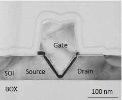 |
| Figure 2: Electron microscope image of the cross-sectional structure of the prototype transistor.
|
|
Figure 3 shows the electrical characteristics of the transistor with a channel length of 3 nm. By changing the gate voltage, the drain current could be modulated over six orders of magnitude or more. Normal current response as a transistor was also confirmed with respect to changes in the drain voltage.
|
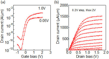 |
| Figure 3: Electrical characteristics of the prototype transistor. (a) Relation between the gate voltage and the drain current. Numbers in the graph indicate the set values for the drain voltage. (b) Relation between the drain voltage and the drain current as the drain voltage was changed to a maximum of 2.0 V in increments of 0.2 V. Normal operation as a transistor was confirmed by these measurements.
|
|
To improve performance of a transistor, its channel thickness is an important parameter. The effects of the thickness at the channel part of the SOI substrate were systematically investigated, and the results are shown in Fig. 4. The conclusion is that achieving a thickness of 1 nm is essential for higher performance. When transistors are miniaturized to the extreme, the structure must be controlled on the nanometer scale.
|
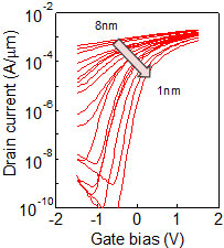 |
| Figure 4: Electrical characteristics when the channel thickness was changed on the nanometer scale. Relations between the gate voltage and the drain current of the transistor with a channel length of 3 nm, made by changing the thickness at the channel part of the SOI substrate. A thickness of 1 nm at the channel part is necessary for higher performance.
|
|
Analyzed velocities of the electrons inside the developed transistor are shown in Fig. 5. The electrons flow at a constant velocity from the source terminal to the drain terminal. In a conventional transistor, the electrons entering the source terminal slow down gradually as they are scattered inside the channel. However, in the transistor with a channel length of 3 nm, the electrons reach the drain with very little scattering, thus keeping the velocity constant. No scattering means no energy loss inside the transistor. The reduction in energy consumption is expected if such transistors are used in future LSIs.
|
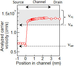 |
| Figure 5: Analyzed electron velocities inside the channel. Electrons entering the source terminal reach the drain without velocity reduction, suggesting that most electrons pass through the channel without scattering.
|
|
Future Plans
|
|
Based on the developed transistor, the researchers plan to expand the research on the transistors of new principle capable of reducing power consumption even further.
|

