| Dec 06, 2013 |
Nanoscale photonic integrated circuit using surface plasmon polaritons on silicon |
| (Nanowerk News) Surface plasmon polaritons (SPPs) are waves that propagate along the surface of a conductor and collective oscillation of electrons coupled with the optical field in the nano-scale area beyond the diffraction limit of propagating light waves. Recently, there is increasing interest in SPPs as signal carriers in nanoscale integrated circuits. |
| Many researchers are developing photonic devices employing SPPs for applications to photonic integrated circuits. |
| Here ("Monolithic Integration of Surface Plasmon Detector and Metal–Oxide–Semiconductor Field-Effect Transistors"), Mitsuo Fukuda and his group at Toyohashi University of Technology (Toyohashi Tech) have developed a nanoscale integrated circuit consisting of SPP and electron devices on silicon in cooperation with the Integrated Circuit and Sensor System Group. |
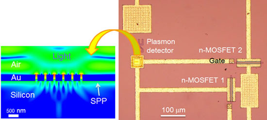 |
| Top view of the integrated circuit (right) and cross sectional view of simulation result for SPP detector. |
| The integrated circuit consists of a SPP detector and two metal-oxide- semiconductor field-effect transistors (MOSFETs). The SPP detector was a gold/silicon Schottky-junction diode with multi-grating slits and fabricated on the gate electrode of a MOSFET. Free electrons excited by SPPs within the gold-metal cross over the junction and result in photocurrent to drive the MOSFET. The SPPs were converted from propagating 1550-nm-wavelength light at the multi-grating slit. |
| The integrated Schottky-junction diode drove the MOSFET well with a 1550-nm- wavelength light beam which is transparent to silicon. The photocurrent detected at the Schottky diode was amplified by about 14000 times in the integrated circuit. |
| This device is expected to contribute to a new phase of nano-scale photonic integrated circuits on silicon. |
| Source: Toyohashi University of Technology |

