| Feb 21, 2014 |
Nanowire and photonic crystal realize a novel optical nanocavity
|
|
(Nanowerk News) Nippon Telegraph and Telephone Corp. (NTT) has developed a novel method to create an optical nanocavity*1 at an arbitrary place on a silicon chip by placing a compound semiconductor nanowire*2 on a silicon photonic crystal*3. This method enables us to integrate a large number of nanophotonic devices based on compound semiconductors on a silicon chip, and is promising for realizing dense optical networks in a processor chip, which is expected to lead to ultrafast information communication technology (ICT) with small power consumption.
|
|
This result have been published in Nature Materials on 20th, Feb. 2014 ("Movable High-Q Nanoresonators Realized by Semiconductor Nanowires on a Si Photonic Crystal Platform").
|
|
Background
|
|
The energy consumption of ICT has been increasing year by year at an accelerated pace, and it is thus strongly demanded to introduce novel technologies to reduce it drastically. As the bit rate goes up, the energy consumption of ICT becomes dominated by electric systems/components, such as routers, data centers and processor chips in them. This is because the electrical signal transport becomes more energy-consuming when the bit rate goes up. This trend is becoming notable even within a processor chip where the most of energy will soon be consumed by electric wirings and on-chip network management.
|
|
To solve this forthcoming problem, It is expected to introduce dense photonic networks into a processor chip in future. This will require technologies to integrate a large number of ultrasmall photonic devices with various functionalities, but the present photonic integration technologies cannot meet this requirement because of the following several reasons:
|
|
i) it is fundamentally difficult to confine light in a small space,
|
|
ii) photonic integration needs to combine different materials to realize required functionalities (though electronic integration are mostly based solely on silicon), and
|
|
iii) present photonic devices consume large amount of energy. In addition, conventional high-performance photonic devices are based on compound semiconductors, such as indium phosphide, though they are incompatible with processor chips which are based on silicon. In order to overcome these difficulties, novel photonic integration technologies have been expected.
|
|
Achievements
|
|
NTT Nanophotonics Center (NPC) located in Atsugi, Japan, has developed a novel photonic integration technology to solve these problems, which is based on a combination of compound semiconductor nanowires and silicon photonic crystals.
|
|
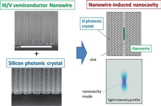
NPC has succeeded in creating an ultrasmall optical cavity by precisely placing a compound semiconductor nanowire with a diameter below 100 nm into a groove on a silicon photonic crystal. Light emission from a nanowire is greatly accelerated as a result of the cavity formation, which proves the strong light confinement achieved in the nanowire.
|
 |
| Idea of this study.
|
|
Since the most of nanophotonic devices consist of optical cavities, the realized structure should be directly applicable to various photonic devices. It is worth noting that there is no cavity in the photonic crystal itself before the nanowire placement, and the cavity is formed only after the nanowire is inserted in the photonic crystal groove. The optical nanocavity is created right at the nanowire position, and it was also confirmed that the nanocavity can be moved if the nanowire is displaced. This method will be applicable to a wide variety of materials if we change the composing materials of nanowires, and various heterostructures can be implemented in the nanowire as well. Since the consumption energy of photonic devices is primarily restricted by their size of the functional region, the present achievement of the strong light confinement into a tiny nanowire shows a promise for ultralow-power photonic devices.
|
|
This method will enable us to integrate a large number of functional nanophotonic devices based on compound semiconductor nanowires at an arbitrary place on a silicon chip, and is promising as a novel photonic integration technology to implement dense photonic network processing functions into a processor chip in future.
|
|
Experiments
|
|
1) A silicon photonic crystal was prepared by semiconductor nanofabrication technology. A compound semiconductor (InAsP/InP) nanowire with a diameter of 90 nm grown by a special crystal growth technique (vapor-liquid-solid method) was placed into a 150-nm-wide groove on the silicon photonic crystal by the nano-probe manipulation technique, as explained below.
|
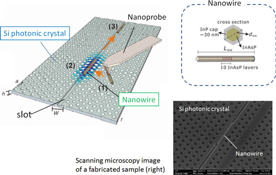 |
| Fabrication with Nanomanipulation.
|
|
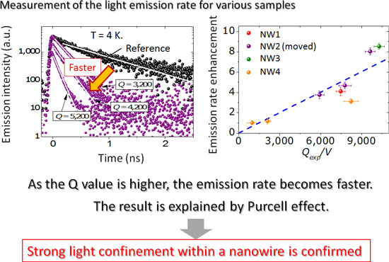
2) The formation of an optical nanocavity was confirmed by the observation of a sharp emission peak in the emission spectrum from the nanowire. The sharp peak appeared only after the nanowire was placed in the Si photonic crystal groove.
|
|
3) As the nanowire was displaced, the optical cavity also moved, which demonstrates the movability of this nanocavity.
|
|
4) We observed that the light emission rate of the nanowire was greatly enhanced after the cavity formation (Purcell effect*4). This confirms the strong light confinement within a nanowire.
|
 |
| Demonstration of Light Confinement.
|
|
Technical Features
|
|
1) Nanocavity formation by a nanowire and a photonic crystal
|
|
A semiconductor nanowire is a novel material grown by the vapor-liquid-solid method. The diameter is typically between 10 to 100 nm, and it is possible to implement various functionalities including heterostructures and a current-injection junction during the growth procedure. Because of these features, nanowires are attracting much attention as promising materials for ultrasmall devices in terms of both of electronics and photonics. However, the performance of nanowire photonic devices has been limited because the size of nanowires is generally too small to realize sufficient light confinement in them.
|
|
A photonic crystal is an artificial material whose refractive index is periodically modulated. Since a photonic crystal is known to function as an optical insulator, which does not exist in nature, extraordinarily strong light confinement is achievable. As a result, a photonic crystal enables an ultrasmall optical cavity, and is expected to be a promising platform for dense photonic integration. However, there is a certain restriction about the composing material, and it is not easy to combine different materials, such as silicon and compound semiconductor, in a single chip. It is also difficult to reduce the size of the functional region.
|
|
In the present achievement, a novel platform consisting of a combination of a compound semiconductor nanowire and a silicon photonic crystal is proposed. The key feature is that this novel combination enables strong light confinement in a functional nanowire with a help of a photonic crystal, in which both of pros are added and cons are eliminated.
|
|
2) Placement of a nanowire by nano-probe manipulation
|
|
We have employed the nano-probe manipulation method to place a nanowire whose diameter is less than 100 nm in a photonic crystal groove. For this method, we displace a single nanowire on a photonic crystal substrate to a certain desired position by scanning a nano-probe equipped in an atomic force microscope system*5.
|
|
Future Plans
|
|
We plan to extend this approach to various nanowires with specific functions, such as optical gain or optical nonlinearity, so as to realize functional photonic devices, such as lasers and optical switches, on a silicon chip. Moreover, we will integrate those nanowire-based photonic devices via waveguides on the silicon photonic crystal platform to form an integrated photonic circuit. In future, we will develop full-fledged large-scale photonic integration technologies with this method together with other nanophotonics technologies. Our goal is to implement dense photonic networks into a processor chip within 10 or 15 years, and to realize ultrafast ICT with drastically-small consumption energy.
|
|
Glossary
|
|
*1 Optical nanocavity - An optical cavity is an element which confines light with a certain resonance. Since it is fundamentally difficult to confine light in a small space, miniaturization of high-performance cavities has been difficult. Historically, small cavities whose size is about 10 to 100 times of the wavelength of light have been called ?microcavities?. Recently, ultrasmall cavities whose size are comparable to the wavelength of light (the volume is less than 1 µm3) is called ?nanocavities?. Various high-performance nanocavities have been realized by employing photonic crystals.
|
|
*2 Semiconductor nanowire - A certain type of semiconductor crystal growth method, known as the vapor-liquid-solid method, can produce very thin wire-like structures whose diameter is 10 to 100 nm. It has been found that a large variety of semiconductors exhibit this growth mode, including compound semiconductors useful for photonic devices. It is possible to implement various functional structures into a nanowire during the growth, such as heterostructures and a current-injection junction.
|
|
*3 Photonic crystal - An artificial structure whose refractive index in periodically modulated by a length scale comparable to the wavelength of light, usually fabricated by semiconductor lithography technology. Since photonic crystals behave as optical insulators, which do not exist in nature, extraordinarily strong light confinement becomes possible and they are therefore expected to realize ultrasmall photonic devices and circuits.
|
|
*4 Purcell effect - E. M. Purcell predicted decades ago that light emission can be accelerated in a wavelength-sized cavity in proportion to the optical field intensity at the emitting material. This effect is expected to enhance the speed and efficiency of light-emitting devices. In addition, this effect can be employed to examine the light confinement strength within the emitter material in the cavity.
|
|
*5 Atomic force microscope - A microscope for measuring the surface shape of a sample by scanning the surface with a nano-probe so as to keep the atomic force between the probe and the sample surface constant. Nanometer resolution is achievable. In this study, the nano-probe equipped in an atomic force microscope is employed for manipulating and displacing a nanowire on the sample surface.
|

