Reference terms from Wikipedia, the free encyclopedia
 

Electromagnetic shielding

In electrical engineering, electromagnetic shielding is the practice of reducing the electromagnetic field in a space by blocking the field with barriers made of conductive or magnetic materials. Shielding is typically applied to enclosures to isolate electrical devices from their surroundings, and to cables to isolate wires from the environment through which the cable runs. Electromagnetic shielding that blocks radio frequency (RF) electromagnetic radiation is also known as RF shielding.

The shielding can reduce the coupling of radio waves, electromagnetic fields, and electrostatic fields. A conductive enclosure used to block electrostatic fields is also known as a Faraday cage. The amount of reduction depends very much upon the material used, its thickness, the size of the shielded volume and the frequency of the fields of interest and the size, shape and orientation of holes in a shield to an incident electromagnetic field.

 
Note:   The above text is excerpted from the Wikipedia article Electromagnetic shielding, which has been released under the GNU Free Documentation License.
 

Check out these latest Nanowerk News:


The interference of many atoms, and a new approach to boson sampling

In new experiments, physicists have used ultracold atoms to demonstrate a new approach to 'boson sampling' - or measuring the pattern of photons that emerge from a maze of mirrors. The findings could help researchers explore the behavior of poorly understood quantum materials.

AI and holography bring 3D augmented reality to regular glasses

Combining advances in display technologies, holographic imaging, and artificial intelligence, engineers have produced a leap forward for augmented reality.

Strictly no dancing

Researchers have discovered a way to stop the quantum dance of atoms 'seen' by electrons in carbon-based organic molecules. This development will help improve the performance of light emitting molecules used in displays and bio-medical imaging.

Atomic-scale telegraphy with light

Physicists manage to reach atomic resolution with optical microscopy by measuring light from a quantum spark faster than a trillionth of a second.

Researchers can now accurately measure the emergence and damping of a plasmonic field

Researchers have developed a new approach to characterize the electric field of arbitrary plasmonic samples, like e.g. gold nanoparticles.

X-ray study offers first look at a quantum version of the liquid-crystal phase

Scientists have achieved the first observation of a state that was only theoretically predicted.

Scientists observe and analyze a phenomenon that combines optical-electrical-mechanical properties in a 2D atomic layer

World's first confirmation of a unique phenomenon combining optical, electrical, and mechanical properties when light is fired at a 2D atomic layer. Can be applied as a 2D nano actuator moving with light.

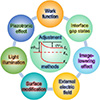
Adjustment methods of Schottky barrier height in one- and two-dimensional semiconductor devices

An international team of scientists presents a comprehensive overview of the static and dynamic adjustment methods of Schottky barrier height, with a particular focus on the recent advancements in nano-semiconductor devices.

Researchers 'unzip' 2D materials with lasers

The new technique can modify the nanostructure of bulk and 2D crystals without a cleanroom or expensive etching equipment.

Tiny displacements, giant changes in optical properties

Materials scientists reveal pathway for designing optical materials with specialized properties.