| Posted: Mar 01, 2010 |
The future of nanoelectronics - transistors without junctions |
| (Nanowerk Spotlight) The first transistors built in 1947 were over 1 centimeter in size; the smallest transistors today are less than 30 nanometers long – over three hundred thousand times smaller. The result of these efforts are billion-transistor processors where a billion or more transistor-based circuits are integrated into a single chip. But this development cannot continue for much longer. One of the increasingly difficult problems that chip designers are facing is that the high density of components packed on a chip makes interconnections increasingly difficult; and, as conventional chip structures continue to shrink, Moore's Law is on a collision course with the laws of physics. |
| All existing transistors are based on junctions – obtained by changing the polarity of silicon from positive to negative. "It is a little bit like changing the color of silicon from black to white," explains Jean-Pierre Colinge, a professor at Tyndall National Institute, whose team has just reported a breakthrough in nanoelectronics by demonstrating the world's first junctionless transistor. |
| "In modern transistors, a negative-positive-negative (black-white-black) structure needs to be created, where the width of the positive (white) region is only a few dozens of atoms wide," continues Colinge, who heads Tyndall's Ultimate Silicon Devices group. "And the coloring has to be done with a paintbrush – it is very difficult to avoid the black paint from smudging into the white region. By contrast, a junctionless transistor is entirely painted white or black. This is much easier to fabricate, especially at very small dimensions." |
| Colinge points out that on the other hand, in a junctionless gated resistor the doping concentration in the channel is identical to that in the source and drain. "Because the gradient of the doping concentration between source and channel or drain and channel is zero, no diffusion can take place, which eliminates the need for costly ultrafast annealing techniques and allows one to fabricate devices with shorter channels." |
| The Tyndall team has reported their findings in the February 21, 2010 online issue of Nature Nanotechnology ("Nanowire transistors without junctions"). |
| "Our devices have full CMOS functionality, but they contain no junctions or doping gradients and are, therefore, much less sensitive to thermal budget issues than regular CMOS devices" Colinge tells Nanowerk. |
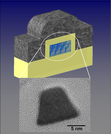 |
| Schematic of a junctionless nanowire transistor (top) and transmission electron micrograph of a single nanoribbon device (bottom). Individual atomic rows can be seen in the silicon. (Image: Dr. Colinge, Tyndall National Institute) |
| "The key to fabricating a junctionless gated resistor is the formation of a semiconductor layer that is thin and narrow enough to allow for full depletion of carriers when the device is turned off" he continues. "The semiconductor also needs to be heavily doped to allow for a reasonable amount of current flow when the device is turned on. Putting these two constraints together imposes the use of nanoscale dimensions and high doping concentrations." |
| The junctionless transistor resembles in a way the first proposed transistor structure, patented in 1928. But so far, no-one had been able to fabricate it – until now. According to the Tyndall team, the key to success was the ability to fabricate silicon nanowires with a diameter of a few dozens of atomic planes, enabled by the electron-beam writing techniques and expertise available at Tyndall. |
| "The electrical current flows in this silicon nanowire, and the flow of current is perfectly controlled by a 'wedding ring' structure that electrically squeezes the silicon wire in the same way that you might stop the flow of water in a hose by squeezing it" explains Colinge. "These structures are easy to fabricate even on a miniature scale which leads to the major breakthrough in potential cost reduction." |
| Semiconductor companies are not only looking at improving the performance of their products, but also at cutting down fabrication costs. The fabrication of sharp junctions for the 22nm node and below require extremely fast, sophisticated and costly annealing techniques. These are no longer necessary in transistors that have no junctions. |
| Another key challenge for the semiconductor industry is reducing the power consumption of microchips. Minimizing current leakage is one of the main challenges in today's complex transistors. "Our junctionless devices have near ideal electrical properties and behave like the most perfect transistors" says Colinge "Moreover, they have the potential of operating faster and using less energy than the conventional transistors used in today s microprocessors." |
| Nevertheless, fabricating these junction-less transistors is not without challenges. The main task is to obtain ultrapure, defect-free silicon crystals with a thickness and a width of a few atoms. This requires the use and control of high-precision instruments like electron-beam lithography equipment and highly skilled operators. |
| Colinge notes that further research will continue with many partners on assessing the prototype's viability for use in the manufacture of silicon chips for electronic devices. The researchers are also beginning to address the issue of variability, which is essential for good industrial process control. |
 By
Michael
Berger
– Michael is author of four books by the Royal Society of Chemistry:
Nano-Society: Pushing the Boundaries of Technology (2009),
Nanotechnology: The Future is Tiny (2016),
Nanoengineering: The Skills and Tools Making Technology Invisible (2019), and
Waste not! How Nanotechnologies Can Increase Efficiencies Throughout Society (2025)
Copyright ©
Nanowerk LLC
By
Michael
Berger
– Michael is author of four books by the Royal Society of Chemistry:
Nano-Society: Pushing the Boundaries of Technology (2009),
Nanotechnology: The Future is Tiny (2016),
Nanoengineering: The Skills and Tools Making Technology Invisible (2019), and
Waste not! How Nanotechnologies Can Increase Efficiencies Throughout Society (2025)
Copyright ©
Nanowerk LLC
|

Become a Spotlight guest author! Join our large and growing group of guest contributors. Have you just published a scientific paper or have other exciting developments to share with the nanotechnology community? Here is how to publish on nanowerk.com. |
