| Posted: Dec 03, 2010 |
Dip-pen nanolithography as EBL alternative for fabricating graphene devices |
| (Nanowerk Spotlight) Dip-Pen Nanolithography (DPN) is a scanning probe lithography technique in which the tip of an atomic force microscope (AFM) is used to deliver molecules to a surface, allowing nanostructured surface patterning on scales of under 100 nm. |
| DPN is the nanotechnology analog of the dip pen where the AFM tip acts as a 'pen', which is then dipped into a molecular 'ink' (i.e. coated with a chemical compound or mixture), and then used to write functional nanoscale patterns by putting it in contact with a substrate, the 'paper'. |
| This direct-write technique offers high-resolution patterning capabilities for a number of molecular and biomolecular 'inks' on a variety of substrates, such as metals, semiconductors, and monolayer functionalized surfaces. It's becoming a work-horse tool for the scientist interested in fabricating and studying soft- and hard-matter on the sub-100nm length scale. |
| Using DPN for fabricating graphene devices has not been previously shown. Researchers at Stanford University have now evaluated DPN as an alternative to conventional electron-beam lithography (EBL) for tailoring such devices. |
| "DPN has several advantages over EBL, such as no damage from electron irradiation and the ability to pattern nanostructures and image them using one system operating under ambient conditions," Maria Wang tells Nanowerk. "We have demonstrated that dip-pen nanolithography can be used to create arbitrarily shaped graphene devices for nanoelectronics and identified the process steps that may affect their electrical characterization." |
| Wang, a PhD graduate of Zhenan Bao's research group at Stanford University, is first author of a recent paper in ACS Nano ("Dip-Pen Nanolithography of Electrical Contacts to Single Graphene Flakes"). This study expanded the tool chest for nanofabrication of graphene devices, thereby making studies of their promising electrical properties accessible to researchers without EBL systems. |
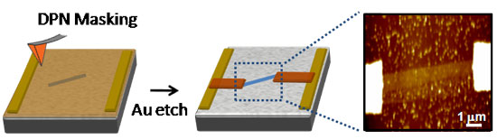 |
| Devices are fabricated using dip-pen nanolithography to isolate a graphene flake and pattern electrical contacts. This patterning of electrical contacts is shown in the schematic above: an atomic force microscopy (AFM) tip is inked with an alkylthiol solution and used to mask parts of the gold film against etching, thereby forming electrical contacts to the graphene flake. An AFM scan reveals the resultant graphene device. (Image: Bao group, Stanford University) |
| The conventional method of fabricating nanoscale devices to explore the unique properties of graphene for electronic applications is electron-beam lithography. However, exposure to electron irradiation may damage the graphene (see our Spotlight: "Just looking at graphene can change its properties"). |
| "In the case of graphene, using DPN to define nanoribbons and other arbitrary nanostructures bypasses the registration limits associated with using a positive resist in EBL" explains Wang. "The goals of our study included evaluating the translation of the DPN process from the 1D carbon nanotube system to the 2D graphene system and characterizing the performance of the resultant devices. The mild processing conditions – lack of electron irradiation – and ease of use and accessibility of AFM systems – as compared to EBL – are strong potential advantages of the DPN approach toward nanodevice fabrication." |
| Wang notes that, since the bulk of this study dealt with exfoliated graphene, DPN replaced two EBL steps: 1) etching these multilayer flakes to isolate monolayer graphene and 2) defining electrical contacts. |
| In order to isolate monolayer graphene from multilayer graphene in exfoliated flakes, the team first identified these monolayer regions optically and then coated the entire flake via thermal evaporation with a 10 nm thick, still continuous gold film. Then, DPN with a surface treatment agent (MHA) masked the gold on top of monolayer graphene, protecting it and leaving the rest of the multilayer graphene flake exposed after gold etching. These exposed multilayers were then removed using an oxygen plasma, which also removes the MHA mask and allows for wet etching of the remaining gold film, thereby revealing the monolayer graphene underneath. |
| In a second DPN masking step, the nanoscale electrical contacts needed to bridge the monolayer graphene flake and the macroscale electrodes were defined. Here, the team used a process that was similar to one that they reported previously for carbon nanotube device fabrication ("Parallel Fabrication of Electrode Arrays on Single-Walled Carbon Nanotubes using Dip-Pen-Nanolithography-Patterned Etch Masks"). |
| The researchers found that the sheet resistance of DPN-generated graphene devices was within the same order of magnitude as reported literature values. Contact resistance and fracture during the gold deposition and etching steps for defining monolayer graphene may have contributed to the slightly higher sheet resistance. |
| "Our results indicate that the fabrication process can cause fracture of some larger graphene flakes, which may be prevented by depositing a protective polymer layer on top of the graphene" says Wang. |
| Wang points out that the DPN process they used is scalable using multipen arrays. "Parallel fabrication of individual graphene devices using DPN could potentially result in higher yield and faster processing times than serial fabrication using EBL. This increase in fabrication efficiency could potentially accelerate graphene research." |
| She also notes that graphene has many interesting physical and electrical properties that have yet to be discovered. "Such fundamental studies require pristine graphene samples; therefore, surface contamination resulting from DPN processing steps, and also seen in some prior reports using EBL, may prevent measurement of intrinsic material properties. Future research needs to be conducted to evaluate the effect of such contamination on measured properties." |
 By
Michael
Berger
– Michael is author of four books by the Royal Society of Chemistry:
Nano-Society: Pushing the Boundaries of Technology (2009),
Nanotechnology: The Future is Tiny (2016),
Nanoengineering: The Skills and Tools Making Technology Invisible (2019), and
Waste not! How Nanotechnologies Can Increase Efficiencies Throughout Society (2025)
Copyright ©
Nanowerk LLC
By
Michael
Berger
– Michael is author of four books by the Royal Society of Chemistry:
Nano-Society: Pushing the Boundaries of Technology (2009),
Nanotechnology: The Future is Tiny (2016),
Nanoengineering: The Skills and Tools Making Technology Invisible (2019), and
Waste not! How Nanotechnologies Can Increase Efficiencies Throughout Society (2025)
Copyright ©
Nanowerk LLC
|

Become a Spotlight guest author! Join our large and growing group of guest contributors. Have you just published a scientific paper or have other exciting developments to share with the nanotechnology community? Here is how to publish on nanowerk.com. |
