| Posted: Feb 16, 2011 |
Monitoring morphological changes during electrodeposition of material with AFM |
| (Nanowerk Application Note) The interaction of objects with their surroundings is largely transmitted over its surface. By application of a coating, the surface properties can be adjusted to protect the object against wear mechanisms such as abrasion or corrosion. Abrasion can be reduced by using a hard coating that can resist high normal or shear forces, or by a coating with lubricating properties. Corrosion can be reduced by coverage of a susceptible metal with a more resistant one, e.g. Nickel. In addition, such coatings can also be applied for cosmetic reasons, e.g. to change the appearance of the surface. One possibility to coat an object with a conducting coating, generally a metal, is electroplating, in which cations from a solution are electrodeposited on it at a suitable potential. At the selected potential, cations of a desired material are reduced from the solution and deposit on the object as a thin layer. Among other factors, the quality of the metal plating will mainly depend on the substrate morphology and the kinetics of deposition. |
| The Cu Damascene electrodeposition[1] in particular is a key fabrication process, currently used in state-of-the-art, multilevel Cu metallization of microelectronic interconnects that range from transistor to circuit board length scale[1,2]. This strongly technology-driven application serves as a key motivator for applied and fundamental mechanistic studies that can spur further development and optimization of the Cu electrodeposition process[3,4]. |
| With an atomic force microscope (AFM) surface morphology can be studied at the nanometer scale. The AFM is not restricted to surfaces in vacuum or air, but can also be used to study the liquid-solid interface. Having the surface wired and incorporated in an electrochemical cell, allows electrochemical reactions at the interface to be provoked and followed functionally by the current flowing through the interface. With the AFM, changes in the surface morphology under these electrochemically relevant conditions can be studied simultaneously. |
| Here we present the reversible electrodeposition, or plating, of a gold surface with copper from a solution containing 1 mM copper sulfate and 100 mM sulfuric acid to increase the electrolyte conductivity. Deposition and dissolution of copper could readily be followed by cyclic voltammetry. The copper-induced morphological changes occurring at the gold surface could simultaneously be recorded by performing AFM measurements in the liquid electrolyte during voltammetry using the Nanosurf FlexAFM, and serves to confirm and better understand the electrochemical process. |
| Experimental setup |
| A conducting sample forms the bottom of the electrochemical cell (see Figures 1a and 1b). A Kel-F cell was mounted on top of the sample and pressed down by a metal plate. To prevent leakage, a 20 mm × 2 mm O-ring made from Kalrez 4079 was present between the sample and the Kel-F cell. |
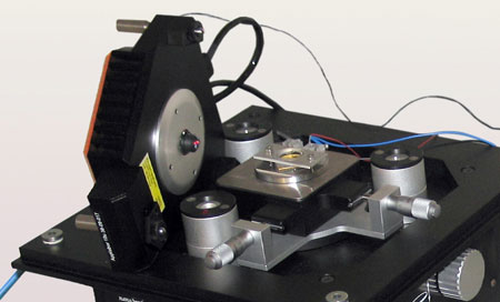 |
| Figure 1a: Experimental Setup. Overview showing the electrochemical cell on a FlexAFM Sample Stage equipped with Environmental Control Chamber, Micrometer Translation Stage and isoStage. The FlexAFm scan head is shown lying on its side, equipped with a Cantilever Holder SA for measurements in liquid. |
| Potentials were set and currents measured with a home-built potentiostat[5]. The substrate was connected to the working electrode of the potentiostat (red wire, center right) via a clamp outside the liquid reservoir. The quasi-reference and counter electrodes (wired blue and black, respectively) enter the liquid over the rim of the reservoir. The reference electrodes used was a copper wire. The counter electrode was made of platinum. The electrolyte solution contained 1 mM CuSO4 and 100 mM H2SO4. All experiments were carried out with a high-resolution FlexAFM scan head equipped with a Cantilever Holder SA for straightforward measurements in liquid environments such as the electrolyte used here. Best image quality was obtained in Dynamic mode (with Phase Contrast data acquisition enabled) using PPP-NCLAuD cantilevers from Nanosensors. |
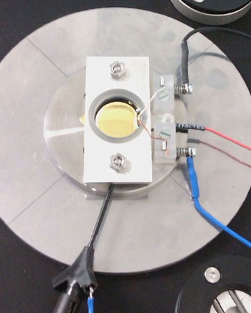 |
| Figure 1b: Experimental Setup. Close-up of the electrochemical cell and the wiring used to connect the electrodes and gold surface. |
| Experimental procedures |
| The sample used in these experiments consisted of a 20 mm × 20 mm glass wafer with gold evaporated onto its surface. The gold was flame-annealed and cooled down under a stream of dry nitrogen. After cooling, the sample was quickly mounted in the electrochemical cell and electrolyte was added. The preferable orientation of the gold film was (111), as concluded from the cyclic voltammograms. Copper deposition and dissolution was carried out as described earlier[4,6–8]. The potential scale on all cyclic voltammograms was zeroed at the equilibrium potential of copper deposition/dissolution in the electrolyte. |
| Results |
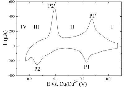
| The upper graph in Figure 2 shows the stepwise deposition and dissolution of a copper monolayer on Au(111) (underpotential deposition, UPD; see ref. 6). The two pairs of current peaks P1/P1'and P2/P2' separate three characteristic potential regions. Region I corresponds to the disordered adsorption of copper and sulfate ions on the gold surfaces. Upon changing the electrode potential past P1, the so-called (√3×√3) honeycomb-type adlayer (region II) is formed, composed of 2/3 copper ion coverage and 1/3 sulfate ion coverage. At more negative potentials than P2 (region III), a full monolayer of copper is formed. These processes are reversible upon positive potential excursion. At potentials more negative than 0.0 V vs. Cu/Cu2+ (reversible Nernst potential) bulk or overpotential deposition (OPD) of copper onto the pre-deposited monolayer takes place in region IV according to a Stranski-Krastanov growth mechanism[6]. |
 |
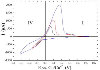 |
| Figure 2: Cyclic voltammograms. Copper deposition (negative peaks) and dissolution (positive peaks) on Au(111) in 0.1 M H2SO4 + 1 mM CuSO4, sweep rate 0.05 V•s-1. (Top) Underpotential deposition and dissolution. (Bottom) Overpotential (bulk) depostion and dissolution in dependence on the turning point at negative potential. |
| From the curves in the lower graph of Figure 2 it can be seen that the amount of bulk deposited copper increases when the turning point (lower left part of the voltammograms) is changed to more negative values. The magnitudes of both the negative deposition and the positive dissolution currents clearly increase. The amount of material can be estimated from the integrated current against time, if other electrochemical processes are neglected. |
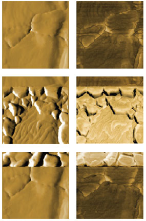 Figure 3: AFM images of bulk deposition and dissolution. Topography (left) and phase (right) of the bare gold substrate (top), the substrate during deposition (middle) and during dissolution (bottom). Topography is displayed as derived data and phase as raw data. Images are 800 nm in size and identically scaled for comparison. Figure 3 shows AFM images of the Au surface recorded before deposition (top), during deposition (middle) and during dissolution (bottom) of copper. The deposition could be confirmed from the change in topography (left), phase (right) and current flowing through the working electrode (gold surface). For the top image of the bare gold, the surface was kept at a positive potential, where no Cu bulk deposition occurs. During recording of the middle images, the voltage was cycled to values E <0.0 V vs. Cu/Cu2+. Images were recorded during the bulk deposition process. Once the 3D phase was nucleated, growth could be observed up to potentials close to 0.0 V vs. Cu/Cu2+. Dissolution of the Cu clusters started at E >0.0 V. The dissolution rate increases with increasing potential. Both deposition and dissolution occur in a very narrow time frame. From the gold surfaces visible in all images, it can be seen that all images were recorded on the same area. All images have a dimension of 800 nm x 800 nm and were scaled identically in Z (morphology: derived data with Sobel filter, center-scaled between -20 and +20; phase: raw data scaled to a 20 degrees range with identical offset). Conclusion The experiment described here demonstrates that electrochemical processes can be elegantly monitored in situ by EC-AFM. To this end, the FlexAFM was equipped with a potentiostat and a special sample holder, suitable for electrochemical experiments. The copper deposition can be steered via the voltage applied by the potentiostat and monitored via the current flowing through the gold substrate. The morphological changes could be recorded during the deposition and dissolution of copper. The experiment serves as proof of concept to study metal deposition, corrosion or other electrochemical phenomena at the nanoscale with EC-AFM. Acknowledgments |
| This work was performed in collaboration with Ilya Pobelov, Artem Mishchenko and Thomas Wandlowski (Department of Chemistry and Biochemistry, University of Bern, Switzerland) and Gabor Meszaros and Tamas Pajkossy (Institute of Materials and Environmental Chemistry, Chemical Research Centre, Hungarian Academy of Sciences, Budapest, Hungary). |
| References |
| 1. Andricacos P, Uzoh C, Dukovic JO, Horkans J and Deligianni H (1998). IBM J. Res. Dev. 42, 567–574. |
| 2. International Technology Roadmap for Semiconductors, 2007 Edition of Interconnect and 2008 Update. |
| 3. Moffat TP, Wheeler D and Josell D in Advances in Electrochemical Science and Engineering, Vol. 10 (Eds.: Alkire RC, Kolb DM, Lipkowski J and Ross PN), Wiley-VCH, Weiheim, 2008, pp. 109–189 and references therein. |
| 4. Kolb DM (1991). Schering Lectures 1, 5. |
| 5. Mészáros G, Li C, Pobelov IV and Wandlowski T (2007). Nanotechnology 18, 424004. |
| 6. Schneeweiss MA and Kolb DM (1999). Phys. Stat. Sol. 173, 51. |
| 7. Pobelov IV, Nagy G and Wandlowski T (2009). J. Chem. Sci. 121, 745. |
| 8. Nagy G and Wandlowski T (2003). Langmuir 19, 10271. |
| Download this application note as pdf: Bulk copper deposition on gold studied in an EC-AFM application using the FlexAFM.pdf. |
| Source: Nanosurf AG |

Become a Spotlight guest author! Join our large and growing group of guest contributors. Have you just published a scientific paper or have other exciting developments to share with the nanotechnology community? Here is how to publish on nanowerk.com. |
