| Posted: Mar 22, 2011 |
CMOS-compatible assembly of semiconducting single-walled carbon nanotube devices |
| (Nanowerk Spotlight) The commercial realization of carbon nanotube-based electronic devices and their integration into the existing silicon-based processor technologies is still hampered by the inability to scale up the – currently lab-based – fabrication processes to manufacture a large number of devices on a single chip. The fundamental issue of carbon nanotube device fabrication still remains the biggest challenge for effective commercialization of nanotube electronics. |
| Two sets of problems are still posing big challenges in developing large-scale single-walled carbon nanotubes (SWCNTs) electronics: 1) The polydispersity of as-grown SWCNTs means that each batch contains a mixture of nanotubes with varied electronic properties; and 2) the high growth temperatures required for SWCNT synthesis – which are incompatible with CMOS technology – rule out directly growing chirality-specific SWCNTs at predetermined locations in an integrated circuit. |
| Applications of sorted SWCNT device arrays (using either metallic or semiconducting SWCNTs) in sensing, MEMS, electronic devices and optoelectronic devices are currently being pursued by research groups around the world. Challenges include being able to produce sorted SWCNT solutions in very large volumes, as well as being able to assemble devices by dielectrophoresis over a large area such as a full wafer. These scalability issues are not fundamental limitations, but engineering challenges, and therefore it is expected that they will be overcome with further research and optimization. |
| Back in 2007, we reported on the directed and precise assembly of single-nanotube devices with an extremely high integration density of more than one million devices per square centimeter, using a novel aspect of nanotube dielectrophoresis (see: "Carbon nanotubes to the rescue of Moore's law"). Research like this has been a big step towards commercial realization of CNT-based electronics and their integration into the existing silicon-based processor technologies. |
| In a further step towards large-scale integration of SWCNTs into complex functional electronic circuits, researchers have now combined their dielectrophoretic deposition approach from 2007 with SWCNT sorting using density gradient ultracentrifugation, ensuring high purity of SWCNTs in suspension and consequently in the assembled devices. |
| "Density gradient ultracentrifugation has been demonstrated ("Sorting carbon nanotubes by electronic structure using density differentiation") by Mark Hersam and co-workers at Northwestern University for separating metallic and semiconducting SWCNTs, and are able to obtain over 99% purity in semiconducting SWCNT solutions," Aravind Vijayaraghavan, a lecturer in Nano Engineering & Storage Technology Research Group at the University of Manchester, explains to Nanowerk. "When this solution is used to deposit SWCNTs by dielectrophoresis, we are able to obtain almost 100% yield in high-density integration of only semiconducting SWCNTs into device arrays." |
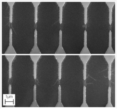 |
| Scanning electron micrograph of 10 adjacent devices from a high-density device array, consisting of only semiconducting SWCNT devices. (Image: Aravind Vijayaraghavan, University of Manchester; Ralph Krupke, Karlsruhe Institute of Technology) |
| This result, reported in the February 25, 2011, online edition of Advanced Materials ("A Scalable, CMOS-Compatible Assembly of Ambipolar Semiconducting Single-Walled Carbon Nanotube Devices"), is important because only semiconducting SWCNTs can be used as devices in microelectronic circuits. This is the first time that it has been shown that large-scale integration is possible with only semiconducting nanotubes at almost 100% yield, and opens the door for wafer-scale production of CNT based devices for electronic applications. |
| In their work, the team, including Ralph Krupke's group at Karlsruhe Institute of Technology, fabricated devices with sorted semiconducting SWCNTs with a mean diameter of 1.4 nm, which is considered optimum for microelectronic applications, on top of a hydrophobic parylene substrate, in order to achieve the desired and expected ambipolar transport. They also demonstrated scalability and integration in arbitrary orientations for the dielectrophoresis assembly route. |
| Another important aspect that the researchers show is that dielectrophoresis is the only way to deposit CNTs in multiple arbitrary directions in a single step, other competing methods such as shear-flow alignment can only deposit unidirectionally, giving more flexibility in chip design. |
| Vijayaraghavan cautions that the as-deposited devices on silicon dioxide do not show the best transport properties, they are unipolar and have low on-state conductance and large hysteresis. |
| "But by assembling the devices on a hydrophobic parylene surface, followed by an annealing procedure, we are able to obtain ambipolar devices, with high on-state conductance and low hysteresis, which are all desirable properties for electronic applications," he says. |
| He notes that the yield of devices corresponds to the purity of the solution, therefore, any further improvement in the percentage of semiconducting tubes in solutions will mean higher yield of semiconducting devices in the array. |
 By
Michael
Berger
– Michael is author of four books by the Royal Society of Chemistry:
Nano-Society: Pushing the Boundaries of Technology (2009),
Nanotechnology: The Future is Tiny (2016),
Nanoengineering: The Skills and Tools Making Technology Invisible (2019), and
Waste not! How Nanotechnologies Can Increase Efficiencies Throughout Society (2025)
Copyright ©
Nanowerk LLC
By
Michael
Berger
– Michael is author of four books by the Royal Society of Chemistry:
Nano-Society: Pushing the Boundaries of Technology (2009),
Nanotechnology: The Future is Tiny (2016),
Nanoengineering: The Skills and Tools Making Technology Invisible (2019), and
Waste not! How Nanotechnologies Can Increase Efficiencies Throughout Society (2025)
Copyright ©
Nanowerk LLC
|

Become a Spotlight guest author! Join our large and growing group of guest contributors. Have you just published a scientific paper or have other exciting developments to share with the nanotechnology community? Here is how to publish on nanowerk.com. |
