| Posted: Jun 27, 2007 |
An ultralow-cost, large area way for nanoelectronics fabrication |
| (Nanowerk Spotlight) Nanoimprinting lithography (NIL) is a simple pattern transfer process that is emerging as an alternative nanopatterning technology to traditional photolithography. NIL allows the fabrication of two-dimensional or three-dimensional structures with submicrometer resolution and the patterning and modification of functional materials. A key benefit of nanoimprint lithography is its sheer simplicity. There is no need for complex optics or high-energy radiation sources with a nanoimprint tool. There is no need for finely tailored photoresists designed for both resolution and sensitivity at a given wavelength. The simplified requirements of the technology allow low-cost, high-throughput production processes of various nanostructures with operational ease. NIL already has been applied in various fields such as biological nanodevices, nanophotonic devices, organic electronics, and the patterning of magnetic materials. Researchers at Berkeley have taken this process one step further by demonstrating that direct nanoimprinting of metal nanoparticles enables low temperature metal deposition as well as high-resolution patterning. This approach has substantial potential to take advantage of nanoimprinting for the application in ultralow cost, large area printed electronics. |
| In nanoimprinting, a mold with nanostructures is pressed to deform and shape a thin material film deposited on a substrate. Therefore, to achieve successful nanoimprinting, the material needs to have proper flow properties (e.g., viscosity and surface tension) adjustable for complete mold pattern replication within reasonable processing temperatures and pressures. Ideal materials usually are thermoplastics, thermoset polymers, or other deformable materials with the desired flow properties. |
| "Nanoimprinting for metals is significantly harder to achieve due to their high melting temperature" Dr. Costas P. Grigoropoulos explains to Nanowerk. "Metal nanoimprinting is typically an indirect process where a polymer (e.g., PMMA) pattern is first created by nanoimprinting, which is then used as mask for dry etching of a predeposited metal film or as part of the metal lift-off process. As one can see, conventional metal nanoimprinting involves multiple steps and expensive processes, thereby increasing the cost of manufacturing and offsetting the advantages of the nanoimprinting process. Very few direct metal nanoimprinting processes have been demonstrated so far due to the high melting temperature of metals." |
| Grigoropoulos, a Professor in Mechanical Engineering at the University of California, Berkeley, together with collaborators from the Berkeley Sensor and Actuator Center as well as UC Berkeley's Department of Chemistry, demonstrates a novel metal direct nanoimprinting method based on the utilization of a metallic material in the form of a nanoparticle solution. |
| "Our process eliminates the need of intermediate polymer nanoimprinting steps for dry etching or vacuum deposition" says Grigoropoulos. "We effectively used a metal nanoparticle solution as a precursor to use the solution processable form of the metal component for the nanoimprinting process, thereby eliminating the need to exceed the bulk metal melting temperature. The nanoimprinted nanoparticles can be transformed into conductive and continuous metal films by low-temperature nanoparticle melting." |
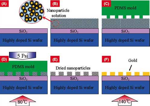 |
Nanoparticle nanoimprinting process. (A, B) Dispensing nanoparticle solution on SiO2/P+ Si wafer. (C, D) Pressing PDMS nanoimprinting mold on nanoparticle solution under 5 psi pressure at 80°C. (E, F) Removal of mold and induce nanoparticle melting on hot plate at 140°C. The magnified view shows the SAM protected nanoparticles suspended in organic solvent. (Reprinted with permission from American Institute of Physics) |
| Combined with an air-stable carboxylate-functionalized polythiophene, the Berkeley team fabricated all solution-processed organic field effect transistors (OFETs) with micrometer to submicrometer critical feature resolution in a fully maskless sequence, eliminating the need for lithographic processes. All processing and characterization steps were carried out at low temperature and ambient environment, which offers a considerable advantage, which will enable further applications to electronics on flexible substrates. |
| In collaboration with ETH, Zurich, Grigoropoulos and colleagues previously have published a string of several papers on the laser-assisted processing of nanoparticle suspensions that demonstrated fabrication of passive (conductors, capacitors) and active (transistors) electronic micro-devices. In a recent paper ("Air stable high resolution organic transistors by selective laser sintering of ink-jet printed metal nanoparticles") they demonstrated laser-enabled OFET fabrication that benefited from the recent development of an air stable carboxylate-functionalized polythiophene that avoids unintentional doping during processing. In the latest paper ("Direct Nanoimprinting of Metal Nanoparticles for Nanoscale Electronics Fabrication"), the researchers now introduce nanoimprinting to achieve nanometric scale devices on flexible substrates. |
| In order to compare the performance of their OFETs, the researchers fabricated reference devices on a thermally grown SiO2 wafer by conventional photolithography and vacuum metal deposition process, and the same semiconducting polymer was spin coated under the same condition. |
| "The overall performance of the lithographically processed OFET with SiO2 dielectric layer exhibited similar performance with our imprinted OFETs" says Grigoropoulos. "This confirms that nanoparticle nanoimprinting can produce similar quality OFETs as conventional photolithography." |
| He notes that the OFET performance can be significantly enhanced by the polymer processing optimization or by applying higher mobility semiconducting polymer. "Direct nanoimprinting utilizes a fully additive method to form electrodes with the desired width and density. It is also worth mentioning that this is accomplished without using expensive photolithographic methods once the nanoimprinting mold is available." |
| Grigoropoulos points out that the methodology presented in this work is scalable and has the potential to lead to massive production of nanolectronics on sensitive substrates. Envisioned applications utilizing this work include chemical and biological sensors and low cost, but high performance electronics for wireless devices and displays. |
| "We intend to push this research to demonstrate reliability, high throughput and low cost" he says. "The materials challenge is always important and has to be addressed from many angles, including the development of semiconducting polymers and new device designs." |
 By
Michael
Berger
– Michael is author of four books by the Royal Society of Chemistry:
Nano-Society: Pushing the Boundaries of Technology (2009),
Nanotechnology: The Future is Tiny (2016),
Nanoengineering: The Skills and Tools Making Technology Invisible (2019), and
Waste not! How Nanotechnologies Can Increase Efficiencies Throughout Society (2025)
Copyright ©
Nanowerk LLC
By
Michael
Berger
– Michael is author of four books by the Royal Society of Chemistry:
Nano-Society: Pushing the Boundaries of Technology (2009),
Nanotechnology: The Future is Tiny (2016),
Nanoengineering: The Skills and Tools Making Technology Invisible (2019), and
Waste not! How Nanotechnologies Can Increase Efficiencies Throughout Society (2025)
Copyright ©
Nanowerk LLC
|

Become a Spotlight guest author! Join our large and growing group of guest contributors. Have you just published a scientific paper or have other exciting developments to share with the nanotechnology community? Here is how to publish on nanowerk.com.
