| Posted: Aug 11, 2011 |
Connecting the dots - fused metal shapes on DNA origami |
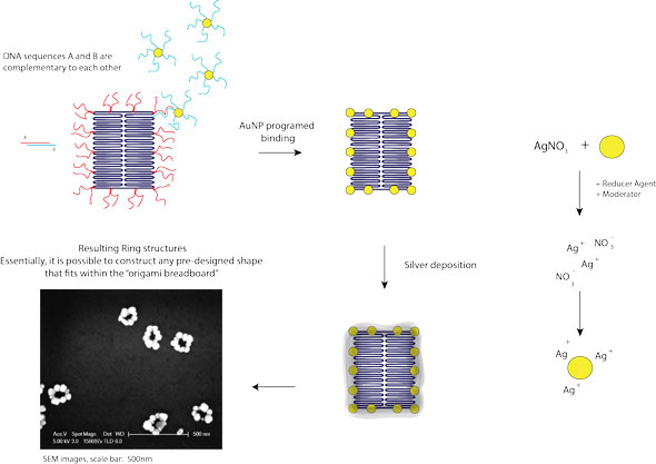
| (Nanowerk Spotlight) 'DNA origami' is a design technique – similar to the traditional Japanese art or technique of folding paper into decorative or representational forms – that is used by nanotechnology researchers to fold DNA strands into something resembling a programmable pegboard on which different nanocomponents can be attached. |
| These DNA assemblies allow the bottom-up fabrication of complex nanostructures with arbitrary shapes and patterns on a ∼100 nm scale. For instance, DNA origami have been heralded as a potential breakthrough for the creation of nanoscale circuits and devices (see "DNA nanotechnology in computers knocks down another roadblock"). |
| DNA can also be metallized with different metals such as gold, copper, platinum or silver, resulting in conducting nanowires (see for instance: "DNA as template for assembling nanostructures"). "However, in those works, the reduced metal coated the entire structure and did not fully utilize the addressability of the underlying DNA template" Gleb Finkelstein, an Associate Professor in the Physics Department at Duke University, tells Nanowerk. "We have developed a method to assemble metallic nanocircuits with arbitrary shapes, by attaching metallic nanoparticles to select locations of the DNA origami and then fusing them to form wires, rings, or any other complex shape. These pre-designed structures are programmed by fully utilizing the self-assembling and recognition properties of DNA." |
| As they have reported in a recent issue of Nano Letters ("Connecting the Nanodots: Programmable Nanofabrication of Fused Metal Shapes on DNA Templates"), by fusing the nanoparticles together, Finkelstein's team has taken the next step toward making electronic circuits on a 100 nm x 100 nm chip. |
| Combining the programmed placement of gold nanoparticles on DNA templates and their fusion by metallization, the team demonstrated that complex metallic nanostructures can be assembled programmatically using DNA templates, DNA functionalization of seed nanoparticles, and metallization via silver reduction chemistry. |
 |
| SEM images of different metallic nanostructures: (A) and (D) H shapes, (B) and (E) pairs of parallel bars, (C) and (F) rings. All scale bars are 500 nm. (Reprinted with permission from American Chemical Society) |
| "We expect that our results will represent an enabling step in fabrication of a wide range of components for nanoelectronic and plasmonic applications," says Finkelstein. |
| Potential applications involve nanoscale electronic and plasmonic circuits – specifically, single molecules detection through plasmonic enhancement, and the bottom-up construction of nanoscale photoelectric devices. The advantage of the DNA self-assembly is its massive parallelism, so that millions of copies are created simultaneously. Even if the yield is not perfect, there will be enough working structures to perform the task. |
| For their work, the Duke team worked with previously reported ("Folding DNA to create nanoscale shapes and patterns") 'tall rectangle' DNA origami (90 x 70 nm2), slightly modified for their purposes, and used it as the DNA template for all of the metallic structures they fabricated. |
 |
| Schematics of the fabrication process. (Credit: Mauricio Pilo-Pais, Duke University) |
| Working with gold nanoparticles, the researchers programmed different binding sites on their DNA scaffolds, resulting in differently patterned assemblies. |
| The researchers note that, while the observed amount of successfully assembled structures appears encouraging, there are many parameters one could still optimize to increase the overall yield even further, among them the design of the binding sites on the DNA origami, the concentrations of the DNA origami and the gold nanoparticle/DNA conjugates, the parameters that control the surface attachment, and the metallization protocol. |
| "Going forward, the main challenge, and the natural next step of our research, is to couple light or electricity to the structures" explains Finkelstein. "Wiring individual structures seems unpractical and could be better done by lithographic techniques. So most probably, we should think of electro-optical solutions, where signals are coupled in and out as light, but the inner working of the structure involves electrical currents." |
 By
Michael
Berger
– Michael is author of four books by the Royal Society of Chemistry:
Nano-Society: Pushing the Boundaries of Technology (2009),
Nanotechnology: The Future is Tiny (2016),
Nanoengineering: The Skills and Tools Making Technology Invisible (2019), and
Waste not! How Nanotechnologies Can Increase Efficiencies Throughout Society (2025)
Copyright ©
Nanowerk LLC
By
Michael
Berger
– Michael is author of four books by the Royal Society of Chemistry:
Nano-Society: Pushing the Boundaries of Technology (2009),
Nanotechnology: The Future is Tiny (2016),
Nanoengineering: The Skills and Tools Making Technology Invisible (2019), and
Waste not! How Nanotechnologies Can Increase Efficiencies Throughout Society (2025)
Copyright ©
Nanowerk LLC
|

Become a Spotlight guest author! Join our large and growing group of guest contributors. Have you just published a scientific paper or have other exciting developments to share with the nanotechnology community? Here is how to publish on nanowerk.com. |
