| Posted: Sep 24, 2013 |
Synaptic electronics |
| (Nanowerk Spotlight) The idea of building bio-inspired cognitive adaptive solid-state devices has been around for decades. It forms the basis for synaptic electronics, a field of research that aims to build artificial synaptic devices to emulate the computation performed by biological synapses. |
| Synapses dominate the architecture of the brain and are responsible for massive parallelism, structural plasticity, and robustness of the brain. They are also crucial to biological computations that underlie perception and learning. Therefore, a compact nanoelectronic device emulating the functions and plasticity of biological synapses will be the most important building block of brain-inspired computational systems (read more: "Brain-inspired computing with nanoelectronic programmable synapses"). |
| In previous Nanowerk Spotlights we have looked at various efforts in neuromorphic engineering – a new interdisciplinary discipline that includes nanotechnologies and whose goal is to design artificial neural systems with physical architectures similar to biological nervous systems (read more: "Nanotechnology's road to artificial brains"). |
| Just recently, for instance, we described research findings where scientists developed a carbon nanotube synapse with the elementary dynamic logic, learning, and memory functions of a biological synapse. |
| The recent revival of interest in building electronic systems that mimic the ability of the brain in performing energy-efficient and fault-tolerant computation in a compact space coincides with the DARPA Synapse program in 2008. Since then, research activities in this field have been growing rapidly. The research effort on brain-inspired computing and synaptic electronics can be understood considering the inefficiency of conventional computational systems in solving complex problems. |
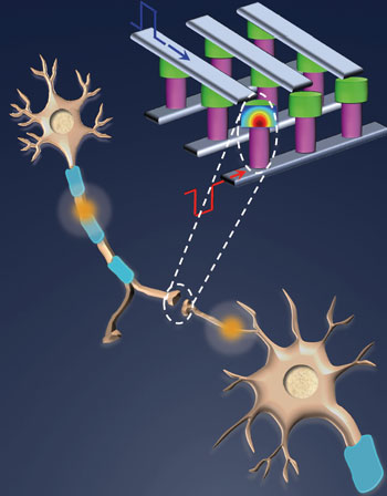 |
| Interconnection scheme of phase-change memory (PCM) synapses to reach ultrahigh density and compactness of brain is shown. In the crossbar array architecture, PCM synapses lie between postspike and prespike electrodes, inspired by biological synapses formed between presynaptic and postsynaptic neurons. The cross sections of depressed (mushroom shaped amorphous region shown in red) and potentiated synapses are shown in the schematic. (Image: Duygu Kuzum, Stanford University) |
| Researchers from H.-S. Philip Wong's Nanoelectronics Group at Stanford University have now published a comprehensive review in Nanotechnology ("Synaptic electronics: materials, devices and applications") that looks at the recent progress of synaptic electronics. In it, they focus on synaptic devices and summarize the important findings and applications published in recent years. |
| They start with a brief description of synaptic plasticity and learning. The different synaptic device implementations are reviewed with an emphasis on materials and switching mechanisms, which is followed by an analysis of the performance metrics. Finally they review targeted computing applications with synaptic devices. |
| However, the authors limit this review to solid-state devices for the emulation of the synaptic functionalities and do not cover the literature on neuromorphic circuits. |
| As the authors point out, the interest in developing synapse-like electronic devices directed attention to material systems that have been investigated for nonvolatile memory technologies. |
| "A broad spectrum of device systems with programmable conductance inspired from already existing device technologies, such as phase change memory (PCM), resistive change memory (RRAM), conductive bridge type memory (CBRAM), ferroelectric switches, carbon nanotube devices, and three terminal devices or FET (field effect transistor) based devices, have been explored. Different material systems or devices have strengths in various characteristics." |
| What are the required characteristics for a synaptic device which will enable the development of brain-inspired systems technology that scales to biological levels of device density, parallelism and functionality? |
| "The synaptic device should be a simple two-terminal nanoscale device in order to reach brain-level parallelism and compactness. The main characteristics are the ones which are directly related to the parallelism, energy efficiency and fault tolerance. The synaptic device should emulate plasticity by implementing an analog-like transition between different conductance states with very low energy consumption per synaptic event. The exact performance metrics depend on the target application and the scale of the system design." |
| The review looks at the research efforts on synaptic devices, categorizing them according to their operation or dominant switching mechanism. One section focuses on passive synaptic devices (phase change, resistive change, conductive bridge, and ferroelectric devices), while another section covers advances in FET-based active synaptic devices. |
| The authors conclude that, although most of the published work focuses on some specific applications for synaptic devices, the field has the potential to be utilized in a broad range of computing applications, especially the ones at the intersection of sensing and computation, where real-time and parallel processing of large-scale data is crucial. |
| "There is an enormous opportunity to completely rethink the design of computational systems in order to gain orders of magnitude of improvement in computational efficiency through inspiration from the biological brain. More interactions among different research disciplines – devices, circuits, architecture, and computing – can further cultivate the synaptic electronics field and help define more targeted research paths for the future." |
 By
Michael
Berger
– Michael is author of four books by the Royal Society of Chemistry:
Nano-Society: Pushing the Boundaries of Technology (2009),
Nanotechnology: The Future is Tiny (2016),
Nanoengineering: The Skills and Tools Making Technology Invisible (2019), and
Waste not! How Nanotechnologies Can Increase Efficiencies Throughout Society (2025)
Copyright ©
Nanowerk LLC
By
Michael
Berger
– Michael is author of four books by the Royal Society of Chemistry:
Nano-Society: Pushing the Boundaries of Technology (2009),
Nanotechnology: The Future is Tiny (2016),
Nanoengineering: The Skills and Tools Making Technology Invisible (2019), and
Waste not! How Nanotechnologies Can Increase Efficiencies Throughout Society (2025)
Copyright ©
Nanowerk LLC
|

Become a Spotlight guest author! Join our large and growing group of guest contributors. Have you just published a scientific paper or have other exciting developments to share with the nanotechnology community? Here is how to publish on nanowerk.com. |
