| Posted: Feb 04, 2014 |
Researchers report revolutionary technique to prepare nanowires (w/video) |
| (Nanowerk Spotlight) Nanostructured boron compounds have attracted considerable scientific attention to exploit their potential use in high temperature electronics, thermoelectrics, and photovoltaics due to their unique properties, such as chemical inertness, hardness, and adjustable energy bandgap. Boron's theoretical tubular structures may even have higher electrical conductivity than carbon nanotubes. Researchers have already demonstrated that boron nanowires have the potential to be excellent field emission nanomaterials or, thanks to their strength, could turn T-shirts into body armor. Furthermore, the high melting temperature of boron (2300°C) together with its lightness (2340 g/cm3) make boron nanowires good material candidates for device components working under extreme conditions, for example, those experienced by spacecraft. |
| "The synthesis of boron based nanostructures usually requires reaction temperatures well above room temperature, and in general, there still remains a lot to be understood on the growth processes of not only boron nanostructures, but nanostructures as a whole," Prof. Mark H. Rümmeli at Sungkyunkwan University in Korea, explains to Nanowerk. "This is because most synthesis approaches are ex situ and inherently provide indirect information. Thus, it is important to compliment ex situ studies with in situ studies." |
| Over the years, researchers have developed a large number of techniques to synthesize nanowires and nanotubes in the laboratory. These procedures vary widely in their hardware requirements and methodology. Nevertheless, they all share a set of common goals: simplicity of protocol; fast execution; and low energy input. |
| Now, an international group of scientists, led by Rümmeli and his team, has reported a breakthrough in all three of these areas, leading to a revolutionary and remarkably simple technique for preparing one-dimensional nanostructures. |
| Reporting their findings in the January 27, 2014 online edition of Nano Letters ("Room Temperature in Situ Growth of B/BOx Nanowires and BOx Nanotubes"), the group demonstrates a unique approach to growing amorphous boron nanowires coated with a thin oxide layer through careful management of the electron beam in a transmission electron microscope (TEM) as it irradiates an amorphous boron oxide matrix embedded with gold nanoparticles. |
 |
| Schematic of the synthesis process. The nanowires are nucleated and continue to grow as long as a sufficiently high current density is provided by the electron beam. The catalyst gold nanoparticles are easily observed at the tip of the nanowires, suggesting they play a direct role in the nanowire growth. (Image: Dr. Rümmeli, Leibniz Institute for Solid State and Materials Research) |
| The technique is entirely carried out at room temperature inside a 'conventional' TEM. It merges two main phenomena to complete the task, namely mass loss through the specimen charging as it interacts with the electron beam, and the catalytic properties of gold nanoparticles at room temperature. |
| As the researchers explain, the entire process is driven by radiolysis reactions due to the irradiating electrons and so does not require an expensive specialized holder or TEM instrument for heating and gas injection. Remarkably high growth rates as high as 7 µm/min, some 50 times higher than observed in CVD growth, are observed for the amorphous coaxial B/BOx nanowires, and this is attributed enhanced surface diffusion of charged boron species due to electrostatic repulsion. Oxygen species are required to activate the gold catalyst nanoparticles, and if insufficient boron is supplied, the catalytic process can use boron from the core of a coaxial nanowire and in the process only leave the outer shell thus forming a BOx nanotube. |
| "Our protocol offers advances on several fronts within the field of nanostructure synthesis," says Rümmeli. "It mainly expands the ranks of room temperature synthesis techniques that are available up to date – mostly electrochemical routes – but it is remarkably simpler and faster than most of them. It also demonstrates yet another powerful nanoengineering feature achieved by a TEM, but It does so by exposing a much more dynamic example than for instance drilling or heating a specimen to change its original structure. Here we are dealing with active controlled growth of nanowires and nanotubes which traditionally was a feature previously reserved for significantly aided or modified TEMs." |
| Of course, as he points out, a key role is played by the specimen composition whose electrical properties must be suitable to promote charge accumulation. Boron oxide possesses the necessary properties, but other semi-metal oxides such as silicon oxide, germanium oxide or even some transition metal oxides (aluminium oxide, zinc oxide) might be up to the task. |
| While, in the present case, the synthesized nanowires are boron-based, the scientists note that they have reasons to believe that the technique could, in principle, be adapted for other material compositions as well. Efforts in this direction are already under way. |
| This novel technique not only allows a high degree of interactive control over the nanowires growth rate and length in real time, it takes the concept of in situ TEM manipulation to a new level. It thus opens up new opportunities to many researchers around the world – who today have 'only' standard, unaided TEMs at their disposition – to join in the controlled manipulation of structures at the nanoscale. |
| In a more particular respect, this technique might take researchers a step closer towards achieving the synthesis of the long sought boron nanotubes. |
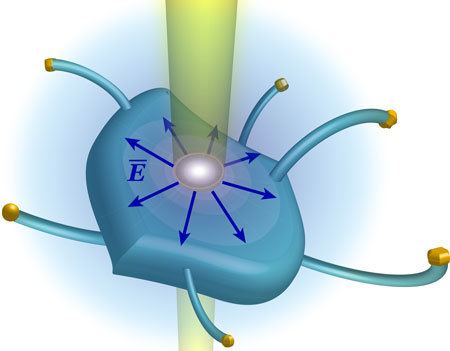
| During the synthesis process, the boron nanowires form overall complex architectures. The nanowires form groups rooted in a central common base and extending radially in all directions, a structure that loosely resembles the traditional picture associated with a neuron. |
| Still frame movie of boron nanowire growth. (Source: Mark H. Rümmeli group, at Sungkyunkwan University) |
| "One can only begin to imagine which kinds of complex networks could be realized if several of these neuron-like structures are made to interact and connect with each other and which set of properties they could display," says Rümmeli. |
| He and his team believe that one of the most straightforward challenges to overcome concerning their novel synthesis technique will be that of its scalability. So far, single groups of nanowires are produced individually, this is not necessarily a disadvantage since it offers interesting possibilities for accurate local experimentation, but, if the goal were to produce nanowires at an industrial scale then the yield would need to be increased by orders of magnitude. Most likely, a new kind of dedicated device would need to be designed to accomplish this challenge. |
| Another challenge would be to find a modification or post-synthesis treatment of the boron oxide nanotubes in order to transform them into pure boron nanotubes. |
 By
Michael
Berger
– Michael is author of four books by the Royal Society of Chemistry:
Nano-Society: Pushing the Boundaries of Technology (2009),
Nanotechnology: The Future is Tiny (2016),
Nanoengineering: The Skills and Tools Making Technology Invisible (2019), and
Waste not! How Nanotechnologies Can Increase Efficiencies Throughout Society (2025)
Copyright ©
Nanowerk LLC
By
Michael
Berger
– Michael is author of four books by the Royal Society of Chemistry:
Nano-Society: Pushing the Boundaries of Technology (2009),
Nanotechnology: The Future is Tiny (2016),
Nanoengineering: The Skills and Tools Making Technology Invisible (2019), and
Waste not! How Nanotechnologies Can Increase Efficiencies Throughout Society (2025)
Copyright ©
Nanowerk LLC
|

Become a Spotlight guest author! Join our large and growing group of guest contributors. Have you just published a scientific paper or have other exciting developments to share with the nanotechnology community? Here is how to publish on nanowerk.com. |
