| Posted: Aug 11, 2016 |
A nanotechnology perspective for manufacturing |
| (Nanowerk Spotlight) The entry of nanotechnology into manufacturing has been compared to the advent of earlier technologies that have profoundly affected modern societies, such as plastics, semiconductors, and even electricity. Applications of nanotechnology promise transformative improvements in materials performance and longevity for electronics, medicine, energy, construction, machine tools, agriculture, transportation, clothing, and other areas. |
| Many technologically sophisticated products today (for example, smartphones, tablet computers, and targeted therapeutic drugs, among many others) already benefit from nanotechnology or some innovative nano-enabled process—as do other products that are not typically conceptualized as 'high tech' such as textiles, lubricants, and athletic gear (Source). |
| However, the path to greater benefits – whether economic, social, or environmental – from nanomanufactured goods and services is not yet clear. A recent review article in ACS Nano ("Nanomanufacturing: A Perspective") by J. Alexander Liddle and Gregg M. Gallatin, takes silicon integrated circuit manufacturing as a baseline in order to consider the factors involved in matching processes with products, examining the characteristics and potential of top-down and bottom-up processes, and their combination. |
| The authors also discuss how a careful assessment of the way in which function can be made to follow form can enable high-volume manufacturing of nanoscale structures with the desired useful, and exciting, properties. |
| Although often used interchangeably, it makes sense to distinguish between nanofabrication and nanomanufacturing using the criterion of economic viability, suggested by the connotations of industrial scale and profitability associated with the word 'manufacturing'. |
| Nanomanufacturing, as the authors define it in their article, therefore, has the salient characteristic of being a source of money, while nanofabrication is often a sink. |
| To supply some background and indicate the scale of the nanomanufacturing challenge, the figure below shows the selling price ($·m-2) versus the annual production (m2) for a variety of nanoenabled or potentially nanoenabled products. The overall global market sizes are also indicated. It is interesting to note that the selling price spans 5 orders of magnitude, the production six, and the market size three. Although there is no strong correlation between the variables, |
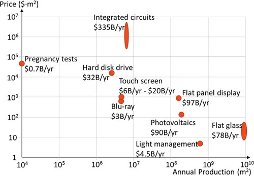 |
| Log-log plot of the approximate product selling price ($·m-2) versus global annual production (m2) for a variety of nanoenabled, or potentially nanoenabled products. Approximate market sizes (2014) are shown next to each point. (Reprinted with permission by American Chemical Society) |
| The term nanomanufacturing covers a wide range of different materials, devices, products, and processes. The term itself can mean making small features on larger objects, (e.g., integrated circuit fabrication); making nanoscale objects with special properties (e.g., quantum dot synthesis); assembling nanoscale objects into more complex structures (e.g., DNA origami-directed assembly); incorporating nanoscale objects into larger objects to enable special functionality (e.g., graphene into electronic devices or into liquor distillation apparatuses); and using nanotechnology to manufacture nanoscale structures (e.g., dip-pen nanolithography). |
| Some of the many nanofabrication techniques under development may one day be used in nanomanufacturing, but, as the authors point out, in order to understand which ones are likely to make the transition to being a revenue source and not a sink, it is necessary to identify how the physical aspects of any given technique affect its ability to generate products that meet the desired functional requirements in a cost-effective manner. |
| The review focuses on nanomanufacturing primarily as it pertains to the creation of structures with a relatively high degree of functionality and structural complexity and hierarchy. It does not address the production of nanomaterials, nor the challenges associated with introducing them into the marketplace. |
| The authors first examine the two broad classes of nanofabrication processes: top-down, i.e., deterministic processes such as photolithography and nanoimprint lithography, and bottom-up, i.e., stochastic processes such as DNA-based self-assembly and colloidal self-assembly. Then, they consider the combination of top-down with bottom-up. Next, they explore what might be possible by adding driven dissipative processes. And finally, they discuss the importance of design for nanomanufacturing. |
| In order to consider the range of products that involve some form of nanomanufacturing, some framework is necessary to enable comparisons between them. In their review, the authors introduce such a framework (which they explain in great detail in their paper): |
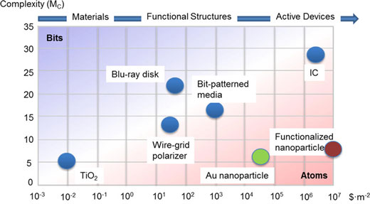 |
| Plot shows a measure of manufacturing complexity, MC, as a function of cost per unit area (dollars per square meter). Manufacturing complexity (MC) is defined as Log10 [Kζmax/(dminf P)], where K is the Kolmogorov complexity; (ζmax/dmin) is a measure of the maximum distance over which spatial coherence must be maintained, compared to the minimum feature size; the fractional tolerance, f, is the maximum allowable variation in feature size; and the perfection, P, is the maximum fraction of defective components or concentration of impurities that can be permitted. The cost may be dominated by the information content (Bits), as in the case of a Blu-ray disk, or by the material (Atoms) as for a protein-functionalized nanoparticle. (Reprinted with permission by American Chemical Society) |
| Although it is notoriously difficult to make predictions about emerging revolutionary technologies like nanotechnology, the authors conclude: " The technology to fabricate integrated circuits will continue to evolve in capability and cost, but will remain uneconomic for low value-per-unit-area, high-volume products. |
| "The family of lithographic technologies, such as nanoimprint, whose development has been driven in large part by the semiconductor industry, will be scaled to suit a variety of cost structures and so will find a wide range of applications, especially for those structures requiring only a single patterned layer. |
| "Bottom-up self-assembly will have a role in the production of simple functional materials that are used in high volumes and must be inexpensive, while directed assembly allows for the imposition of longer-range order and hierarchy that will be important for some applications. |
| "Perhaps the most exciting prospect is that of creating dynamical nanoscale systems that are capable of exhibiting much richer structures and functionality. Whether this is achieved by learning how to control and engineer biological systems directly, or by building systems based on the same principles, remains to be seen, but will undoubtedly be disruptive and quite probably revolutionary." |
 By
Michael
Berger
– Michael is author of four books by the Royal Society of Chemistry:
Nano-Society: Pushing the Boundaries of Technology (2009),
Nanotechnology: The Future is Tiny (2016),
Nanoengineering: The Skills and Tools Making Technology Invisible (2019), and
Waste not! How Nanotechnologies Can Increase Efficiencies Throughout Society (2025)
Copyright ©
Nanowerk LLC
By
Michael
Berger
– Michael is author of four books by the Royal Society of Chemistry:
Nano-Society: Pushing the Boundaries of Technology (2009),
Nanotechnology: The Future is Tiny (2016),
Nanoengineering: The Skills and Tools Making Technology Invisible (2019), and
Waste not! How Nanotechnologies Can Increase Efficiencies Throughout Society (2025)
Copyright ©
Nanowerk LLC
|

Become a Spotlight guest author! Join our large and growing group of guest contributors. Have you just published a scientific paper or have other exciting developments to share with the nanotechnology community? Here is how to publish on nanowerk.com. |
