| Posted: Aug 16, 2016 |
Moire Nanosphere Lithography allows fabrication of large-area tunable graphene metasurfaces |
| (Nanowerk Spotlight) Graphene, one of the most exciting two-dimensional (2D) materials, has shown extraordinary optical properties due to strong surface plasmon polaritons supported by the graphene nanostructure. Graphene metasurfaces show plasmonic resonance bands that can be tuned from mid-infrared (MIR) to terahertz (THz) regime. These plasmonic devices can be used for biosensing, spectroscopy, light modulation and communication applications. |
| Commonly fabricated graphene plasmonic metasurfaces are usually single-band. Plasmonic metasurfaces with multi-band resonance peaks have proven to be extremely effective in molecular detection with ultrahigh sensitivity and accuracy. Multi-band devices at variable electromagnetic spectra are also highly desired to meet the strong demand for the ever-increasing accuracy and high speed in surveillance and communication systems. |
| Researchers at the University of Texas at Austin, led by professors Yuebing Zheng and Deji Akinwande, demonstrate for the first time an effective method to pattern large area graphene – which is grown by chemical vapor deposition (CVD) – into moiré metasurfaces with gradient nanostructures having multiband resonance peaks in mid infrared range (MIR). |
| The results of this work have been published in the August 11, 2016 online edition of Advanced Optical Materials ("Tunable Graphene Metasurfaces with Gradient Features by Self-Assembly-Based Moiré Nanosphere Lithography"). |
| "In our work, the CVD graphene is patterned into moiré metasurfaces via combination of moiré nanosphere lithography (MNSL) with O2 reactive ion etching (RIE)," Zilong Wu, researcher at University of Texas at Austin, paper’s first author, tells Nanowerk. "In brief, colloidal polystyrene (PS) nanospheres self-assemble into monolayer on substrates with graphene. A second monolayer of PS nanospheres is then deposited on top of the first PS monolayer via a similar process." |
| Wu explains that the relative rotation angle between the first and second PS monolayer can be controlled to obtain various moiré patterns. The following RIE with O2 creates voids between closely packed nanospheres and etches away graphene that are exposed to O2 plasma by voids. |
| After removal of the residue nanospheres, graphene sheets with moiré patterns are then left on substrates. |
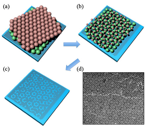 |
| (a-c) Schematics of fabrication processes of graphene moiré metasurfaces on Si substrates (blue). θ denotes the relative rotation angle between the bottom (green) and top (red) monolayers of nanospheres. (d) SEM figures of a representative graphene moiré metasurface. (Reprinted with permission by Wiley-VCH Verlag) (click on image to enlarge) |
| "By varying the relative rotational angle between top and bottom monolayers of PS nanosphere during MNSL, the size and shape of the graphene nanostructures in the metasurfaces change significantly," Wu adds. |
| Wei Li, the paper’s joint first author, points out "that our results demonstrate that graphene moiré metasurfaces with gradient and complex moiré patterns can be controllably fabricated in cost effective and scalable way." |
| Maruthi Yogeesh, a graduate student in Prof. Akinwande's research group, and a co-author of the paper working on FTIR characterization of these graphene metasurfaces, notes that these devices support surface plasmon with resonance wavelength that is highly dependent on the shape and size of the nanostructures. |
| "Under light illumination, the surface plasmon resonances can be excited. Due to the large gradient and the high complexity of graphene moiré metasurfaces, they are promising candidates for tunable multiband plasmonic devices," he says. "We prove this by measuring the transmission extinction of graphene moiré metasurfaces with different patterns. The number and the wavelength of resonance peaks of the graphene metasurfaces are highly dependent on the patterns." |
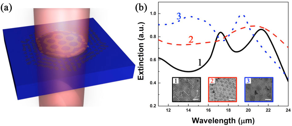 |
| (a) Schematic illustration of transmission extinction measurement of graphene moiré metasurfaces. The graphene nanostructures illuminated by incident light are excited to support surface plasmon resonances, resulting extinction in transmission. (b) Measured extinction spectra of three graphene moiré metasurfaces with different patterns. (Reprinted with permission by Wiley-VCH Verlag) |
| "We have demonstrated large-area graphene moiré metasurfaces by MNSL," Prof. Zheng concludes. "Our studies reveal that the extinction spectra of the graphene metasurfaces can be controlled by the size and shape of the graphene nanostructures. We also demonstrate for the first time multiband graphene metasurfaces in mid infrared range by the complex and gradient nanostructures in moiré patterns”. |
| "These tunable and multiple plasmon resonance modes in the MIR and THz range of electromagnetic spectra make graphene moiré metasurfaces very promising candidates for ultrathin light modulators, biosensors, flexible optoelectronics and photodetectors," says Prof. Akinwande (who recently received the prestigious presidential early career award (PECASE) for his group's outstanding work on two dimensional (2D) materials based electronics). |
| In previous Nanowerk Spotlights we covered the work of Akinwande's research group on "Flexible, low-power, high-frequency nanoelectronics with monolayer MoS2" as well as graphene-based smart contact lenses that work as self-powered biosensor. We covered Prof. Zheng's previous work on bubble-pen lithography and earlier work on Moiré Nanosphere Lithography. |
 By
Michael
Berger
– Michael is author of four books by the Royal Society of Chemistry:
Nano-Society: Pushing the Boundaries of Technology (2009),
Nanotechnology: The Future is Tiny (2016),
Nanoengineering: The Skills and Tools Making Technology Invisible (2019), and
Waste not! How Nanotechnologies Can Increase Efficiencies Throughout Society (2025)
Copyright ©
Nanowerk LLC
By
Michael
Berger
– Michael is author of four books by the Royal Society of Chemistry:
Nano-Society: Pushing the Boundaries of Technology (2009),
Nanotechnology: The Future is Tiny (2016),
Nanoengineering: The Skills and Tools Making Technology Invisible (2019), and
Waste not! How Nanotechnologies Can Increase Efficiencies Throughout Society (2025)
Copyright ©
Nanowerk LLC
|

Become a Spotlight guest author! Join our large and growing group of guest contributors. Have you just published a scientific paper or have other exciting developments to share with the nanotechnology community? Here is how to publish on nanowerk.com. |
