| Posted: Jan 06, 2016 |
Flexible, low-power, high-frequency nanoelectronics with monolayer MoS2 |
| (Nanowerk Spotlight) Molybdenum disulfide (MoS2), an abundant mineral that often is used in steel alloys or as an additive in lubricants, increasingly is being studied for use in nanoelectronics. This semiconducting material exhibits unique physical, optical and electrical properties correlated with its single-layer atomic layer structure. Important for electronics applications, and in contrast to graphene, MoS2 has a bandgap. |
| In the past, the performance of synthesized MoS2 had been poor, especially when integrated on flexible substrates. A new study has now yielded the highest performance for CVD-grown monolayer MoS2 device properties on flexible substrates to date. |
| Reporting their findings in the December 28, 2015 online edition of Advanced Materials ("Large-Area Monolayer MoS2 for Flexible Low-Power RF Nanoelectronics in the GHz Regime"), a team from The University of Texas at Austin has demonstrated for the first time highly flexible and robust CVD monolayer MoS2-based radio frequency (RF) transistors operating at GHz range. |
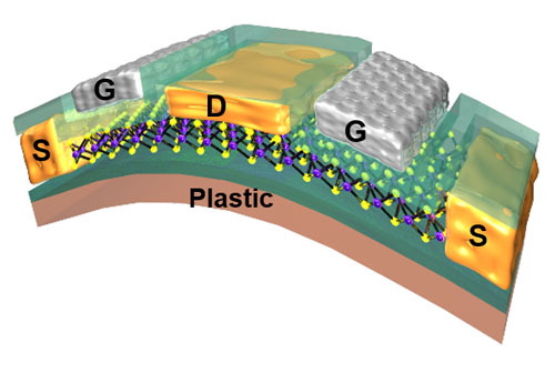 |
| Schematic of the CVD-grown MoS2 FET device. (Image: Jo Wozniak/Deji Akinwande, The University of Texas at Austin) |
| "Our advance has been made possible by improvements in MoS2 synthesis, transfer and device integration onto plastics," Maruthi Nagavalli Yogeesh, a PhD student in Prof. Deji Akinwande's research group, explains to Nanowerk. "Particularly important is that we discovered that the electrons in MoS2 can travel at high velocities sufficient to afford GHz frequencies." |
| The team's discovery is important because it demonstrates that MoS2 is a higher-performance material compared to conventional thin-film transistors made from organic semiconductors, metal oxides or amorphous silicon devices. |
| The demonstration of large-area (millimeter-scale) monolayer MoS2 based flexible RF transistors operating at GHz performance is very promising for the design of low-power and high-frequency flexible RF nanoelectronics systems for the emerging field of wearable systems and Internet of Things. |
| For their monolayer MoS2 devices, the team employed a CVD process on SiO2/Si. They then used a PMMA supported wet transfer process to transfer the resulting monolayer MoS2 onto various substrates. |
| They then fabricated flexible MoS2-based RF transistors which show the highest intrinsic cutoff frequency (ft) of 5.6GHz and power gain (fmax) of 3.3GHz. |
| "These numbers imply that flexible MoS2 transistors can be fabricated over large plastic sheets and offer wireless connectivity at common cellular and bluetooth bands," Akinwande points out. "To this end, we have successfully demonstrated the circuit building blocks for mobile communication systems: amplifier, mixer and wireless AM receiver. In addition, our transistors are mechanically robust enduring 10,000 bending cycles." |
| The team's immediate next goal is to demonstrate novel flexible wireless radio systems based on their MoS2 FETs. |
| "There are many challenges ahead, like how to successfully integrate different building blocks of RF systems like antennas, amplifiers and mixers," says Yogeesh. "We are also exploring how to successfully fabricate passive (inductors, capacitors and resistors) and active components (transistors) simultaneously on flexible platform." |
 By
Michael
Berger
– Michael is author of four books by the Royal Society of Chemistry:
Nano-Society: Pushing the Boundaries of Technology (2009),
Nanotechnology: The Future is Tiny (2016),
Nanoengineering: The Skills and Tools Making Technology Invisible (2019), and
Waste not! How Nanotechnologies Can Increase Efficiencies Throughout Society (2025)
Copyright ©
Nanowerk LLC
By
Michael
Berger
– Michael is author of four books by the Royal Society of Chemistry:
Nano-Society: Pushing the Boundaries of Technology (2009),
Nanotechnology: The Future is Tiny (2016),
Nanoengineering: The Skills and Tools Making Technology Invisible (2019), and
Waste not! How Nanotechnologies Can Increase Efficiencies Throughout Society (2025)
Copyright ©
Nanowerk LLC
|

Become a Spotlight guest author! Join our large and growing group of guest contributors. Have you just published a scientific paper or have other exciting developments to share with the nanotechnology community? Here is how to publish on nanowerk.com. |
