| Posted: Apr 21, 2006 |
Fabricating palladium nanostructures in a simple and inexpensive way |
| (Nanowerk News) Researchers in Canada used the electroless deposition process for self-assembling palladium nanostructures, such as wires, from nanoparticles on a rough stainless steel substrate. This discovery holds a lot of potential for various engineering applications because the deposition process and the preparation of the substrate are simple and inexpensive. |
| In general, metal nanostructured materials, such as nanoparticles, nanowires and nanoarrays have attracted much attention due to their extraordinary electronic, optical and chemical properties. Palladium (Pd) nanowires receive a lot of attention from researchers as an ideal material for H2 sensing because Pd selectively absorbs H2 gas. For more details, see our Nanowerk Spotlight of March 15, 2006: "In the future hydrogen economy, nanotech-based H2 sensors will be widely needed". |
| The most common synthetic methods such as electrochemical and vapor depositions have been successfully used to develop high quality arrays of nanostructures in a large variety of materials. The Canadian researchers now, for the first time, used the electroless deposition process to create Pd nanowires. Electroless deposition occurs simply by immersion of samples in a plating bath and does not need rectifiers, batteries or anodes. The deposition of palladium is an autocatalytic process. |
| First author Zhongliang Shi together with Jerzy Szpunar, both from the Department of Mining, Metals and Materials Engineering at McGill University in Montreal, and Shanqiang Wu from AH2T Inc. in Montreal, reported their new findings in an article titled "Self-assembled palladium nanowires by electroless deposition" published online on March 31, 2006 in Nanotechnology. Their latest report follows an earlier article where they report " Synthesis of palladium nanostructures by spontaneous electroless deposition", published online on March 10, 2006 in Chemical Physics Letters. |
| "Based on our systematic experiments, we find that the diameter of palladium nanowires can be controlled by the electroless deposition process" says Shi. Shi and his colleagues note that "it is generally accepted that electroless deposition of palladium on conductive media is random, spontaneous and uniform as this process has been often used for depositing dense Pd membranes on various substrates." |
| The researchers reasoned that, if nucleation and growth of metal nanograins are controlled by diffusion, the nanograins may connect to each other in order to minimize their surface energy. |
| "So far, there has been no report on metal nanowires assembled without any external field because it is difficult to control the transient time of nucleation and growth in one direction" says Shi. |
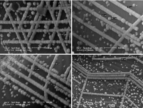 |
| SEM micrographs showing the network structures of self-assembled palladium nanowires on the surface of porous stainless steel substrate by electroless deposition (deposition time: 120 s). (Source: Zhongliang Shi, McGill University) |
| The researchers found that the structures of Pd nanowires are assembled from its nanoparticles bead-by-bead. The nanoparticles link to each other in a certain order and then the neck between the particles disappears. This assembly results only from the autocatalytic reaction in a very short deposition time without any external field. |
| "Another interesting structure is the Pd nanowires network" says Shi, "where a simple node links two palladium nanowires well. The Pd nanowires are well self-organized and it seems that the reduction of surface free energy is the main driving force for aligning the nanoparticles to highly ordered wire and reducing the interface between them." |
| The researchers are now in the process of developing these special PD structures, from single wire to network, for engineering application. Methods are being explored to extract the nanowires from the substrate and to manufacture the nanowires on other substrates which can easily be integrated directly with some microdevices. The possibility of processing other metal nanowires, made of Cu, Ni, Au and Co, in a self-assembled manner using the same approach is also being investigated. |
 By
Michael
Berger
– Michael is author of four books by the Royal Society of Chemistry:
Nano-Society: Pushing the Boundaries of Technology (2009),
Nanotechnology: The Future is Tiny (2016),
Nanoengineering: The Skills and Tools Making Technology Invisible (2019), and
Waste not! How Nanotechnologies Can Increase Efficiencies Throughout Society (2025)
Copyright ©
Nanowerk LLC
By
Michael
Berger
– Michael is author of four books by the Royal Society of Chemistry:
Nano-Society: Pushing the Boundaries of Technology (2009),
Nanotechnology: The Future is Tiny (2016),
Nanoengineering: The Skills and Tools Making Technology Invisible (2019), and
Waste not! How Nanotechnologies Can Increase Efficiencies Throughout Society (2025)
Copyright ©
Nanowerk LLC
|

Become a Spotlight guest author! Join our large and growing group of guest contributors. Have you just published a scientific paper or have other exciting developments to share with the nanotechnology community? Here is how to publish on nanowerk.com.
