| Posted: May 01, 2018 |
A nano squeegee to clean nano sheets |
| (Nanowerk Spotlight) Two-dimensional (2D) materials represent the ultimate scaling-down of materials because 2D materials are only a single molecular layer thick. One type of materials that nanotechnology researchers are particularly interested in is called van der Waals heterostructures – assemblies of artificially stacked 2D layers of different materials. |
| By precisely stacking various 2D materials in a predetermined sequence on top of each other, researchers can create materials that, due to their unique interlayer coupling, have special optoelectronic properties; which makes them of considerable interest for next-generation nanoelectronics and other unique devices. |
| Unfortunately, the study of 2D monolayers is plagued by trapped contaminants in between the 2D sheets as well as between the 2D sheets and the underlying substrate. These contaminants make it difficult to obtain precise and reproducible experimental observations. |
| This means that, when conducting investigations, scientists don't know whether they are measuring the intrinsic material behavior or the interaction of the material with the contaminants. And that, of course, impacts the investigations of the fundamental physics of these materials. |
| Clean and homogeneous interfaces are critical for van der Waals heterostructures and any trapped contaminants between 2D layers is leading to poor interface quality. A clean interface reduces the interlayer spacing (which increases interlayer coupling) and leads to a reduction in externally induced heterogeneity caused by trapped contaminants between layers. |
| New findings, reported in ACS Applied Materials & Interfaces ("Nano-'Squeegee' for the Creation of Clean 2D Material Interfaces") by a team of scientists from the U.S. Naval Research Laboratory (NRL), present a simple technique for removing these contaminants in a process similar to a squeegee, which enables unambiguous investigation of the intrinsic properties of monolayer 2D materials. |
| The below figure illustrates the operating concept of the AFM flattening technique that the team developed, in which the tip of an atomic force microscope (AFM) squeezes out contaminants trapped between the 2D layer and the substrate: |
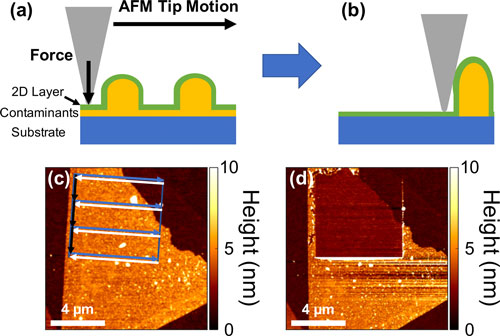 |
| (a, b) Cartoon illustrating the general concept of AFM flattening. After mechanical transfer, there are contaminants trapped between the 2D layer and the substrate, which are often a combination of a uniform thickness layer and bubbles as shown in (a). Applying a normal load with the AFM tip pushes the contaminants out from beneath the tip and induces direct contact between the 2D layer and the substrate. Scanning the tip across the surface while applying normal load causes the contaminants to collect into a pocket, leaving behind a region without contaminants as shown in (b). (c) AFM topography of mechanically transferred CVD WSe2 on hBN. The arrows show the general raster pattern used to flatten an area. Starting from the top left corner, the AFM tip scans to the right (blue arrows) and the left (white arrows), and then the tip moves down between each scan line (black arrows). (d) AFM topography after flattening a 6 µm × 6 µm area of the WSe2 sample. (Reprinted with permission by American Chemical Society) |
| "Clean and homogeneous interfaces are essential for understanding and leveraging the unique physics of 2D materials," Matthew Rosenberger, a National Research Council Postdoctoral Fellow at NRL and the paper's first author, tells Nanowerk. "This has been well known for many years, but it remains challenging to actually obtain clean interfaces in practice. Our work advances the field of 2D materials because we have developed a simple technique for achieving such clean and homogeneous 2D material interfaces, which will aid other researchers in understanding the intrinsic behaviors of 2D materials." |
| He adds that a necessary condition for successful AFM flattening is that the adhesion between the 2D material and the substrate must be sufficient to prevent contaminants from migrating back between the 2D layer and the substrate after removal of the AFM tip. |
| In their experiments, the team found that this is not always the case. It appears that substrate surface roughness plays an important role in the adhesion between a 2D layer and the substrate. |
| The team's findings should be of interest for other research teams because they have demonstrated a simple technique for creating clean 2D material interfaces using only an atomic force microscope, which is a common instrument in the field of 2D materials. |
| Although this technique can't facilitate large-throughput that is required for industrial-scale processes, it is a new approach for gaining a better understanding of the behavior of 2D materials; an essential prerequisite for developing real-world technologies. |
| "The primary next stage in our investigations will be to utilize the squeegee technique on many types of 2D material samples in order to gain insight into the fundamental physics of these materials," Rosenberger concludes. "Understanding these fundamental physics will help us to design better technologies that are relevant to the Navy, such as wearable and stretchable electronics and cost-effective chemical and biological sensors." |
 By
Michael
Berger
– Michael is author of four books by the Royal Society of Chemistry:
Nano-Society: Pushing the Boundaries of Technology (2009),
Nanotechnology: The Future is Tiny (2016),
Nanoengineering: The Skills and Tools Making Technology Invisible (2019), and
Waste not! How Nanotechnologies Can Increase Efficiencies Throughout Society (2025)
Copyright ©
Nanowerk LLC
By
Michael
Berger
– Michael is author of four books by the Royal Society of Chemistry:
Nano-Society: Pushing the Boundaries of Technology (2009),
Nanotechnology: The Future is Tiny (2016),
Nanoengineering: The Skills and Tools Making Technology Invisible (2019), and
Waste not! How Nanotechnologies Can Increase Efficiencies Throughout Society (2025)
Copyright ©
Nanowerk LLC
|

Become a Spotlight guest author! Join our large and growing group of guest contributors. Have you just published a scientific paper or have other exciting developments to share with the nanotechnology community? Here is how to publish on nanowerk.com. |
