| Posted: Mar 26, 2008 |
Nanophotonic structures suitable for CMOS compatible technologies |
| (Nanowerk Spotlight) The success of the computer and communications industry is mainly due to the possibility of a large volume and low cost production output: silicon wafers containing myriad micro and nano structures are at the basis of Complementary Metal Oxide Semiconductor (CMOS) technology. |
| A challenge is the realization of spatially ordered nanostructures in silicon that have many interesting applications like photonic crystals to mod the flow of light, chemical sensors, devices to alter the wetting of liquids on a surface, and as capacitors in high-frequency electronics used in mobile phones. The incorporation of such structures on existing silicon chips is greatly desired, and adapting conventional semiconductor nanofabrication to that end is widely pursued. |
| Just a few days ago we wrote about the general aspects and challenges of silicon photonics and today we are taking a look at a specific fabrication challenge. |
| The challenge for researchers is to to obtain photonic crystals with stop bands in the telecommunication wavelength regions, i.e.1330 nm and 1550 nm. To do that, the diameter of these pores must be smaller than 500 nm. The pore to pore distances, also referred to as pitch or interpore distance, must be well below 1 µm. Furthermore the depth to diameter aspect ratio of the pores must be as high as possible to obtain photonic crystals with large enough volumes. |
| Researchers in The Netherlands now have demonstrated a method to etch arrays of nanopores in silicon with record depth-to-diameter ratios. These structures are suitable for nanophotonics and were made completely with CMOS compatible technologies, making integration of photonic structures in silicon chips feasible. |
| "Several techniques have been developed for the formation of arrays of nanopores in silicon" Léon Woldering tells Nanowerk. The electrochemical etching of pores is a beautiful example of a fabrication technique for photonic crystals made by etching. Although structures with impressive aspect ratios have been obtained, this technique is quite complicated and uses non-standard equipment, and is therefore not likely to be incorporated in CMOS semiconductor nanofabrication. Silicon double inversion is another interesting method to realize pores with high aspect ratios. However, this method is rather complex since it requires many preparative steps, including non-CMOS equipment. Since the reported transmittance for wavelengths around 1.5 µm is rather low, the technique seems less suited for making photonic structures with bandgaps in the telecommunication windows." |
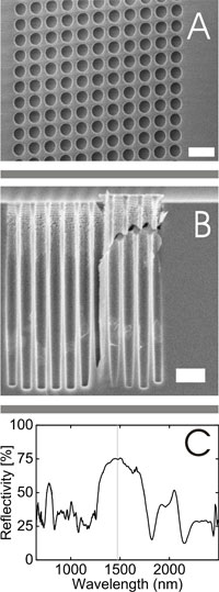 |
| A) Scanning electron micrograph of an array of pores made by deep UV lithography. The diameter of the holes in the pattern equals 462 nm. The distance between the holes equals 600 nm. The scale bar equals 1 µm. B) A cross-section of deeply etched pores. These have a diameter of 423 nm and a high aspect ratio of 15.2. The apparent irregularity on the right side is due to cleaving of the sample. The scale bar equals 1 µm. C) Optical reflectivity measurement of an array of nanopores that demonstrates photonic crystal behavior. The peak at 1471 nm is the first order stop band. (Images: Léon Woldering, University of Twente) |
| Woldering is a member of the Complex Photonic Systems Group (COPS) in the Faculty of Science and Technology at the University of Twente in The Netherlands and first author of a recent paper in Nanotechnology that describes a novel reactive ion etching method to fabricate deep nanopores with high aspect ratios (Periodic arrays of deep nanopores made in silicon with reactive ion etching and deep UV lithography) |
| Together with Willem Tjerkstra and Willem Vos from COPS, Henri Jansen from MESA+ Institute for Nanotechnology, and Irwan Setija from ASML Veldhoven, the Dutch team has fabricated many arrays of myriad nanopores. |
| The researchers defined the structures by means of a mask that was made using advanced deep UV lithography: A giant photo camera, using deep UV light, precisely imaged the structures in a photoresist. Much effort was geared to optimizing the plasma etching method that is also used in industry, in order to obtain very deep nanopores. |
| "We found that minimizing the sidewall erosion is crucial to improve the maximum aspect ratio of the pores, which is the ratio of depth to diameter" explains Woldering. "In this fashion a record aspect ratio of more than 16 was achieved. To the best of our knowledge, this is the highest aspect ratio ever reported for arrays of nanopores in silicon made with a reactive ion etching process." |
| This enables the fabrication of photonic crystals with large volumes, which also opens an avenue towards the fabrication of three-dimensional crystal structures. |
| The researchers also show that reducing the sidewall erosion is the best way to maximize the aspect ratio of their sub-micrometer structures. Increasing the etching rate has a far less significant effect. |
| Woldering points out that In optical reflectivity experiments, they found that the novel structures behave as high-quality photonic crystals with broad forbidden bands in the telecommunications ranges near 1330 and 1550 nm. |
| "The availability of arrays of such deep nanopores with a large range of pore diameters – 310 to 515 nm – and of pitches – 440 to 750 nm – opens an avenue towards the fabrication of three-dimensional photonic crystals that provide ultimate control of the behavior of photons" he says. "We believe that our CMOS-compatible fabrication process is compatible with nanophotonic applications." |
| In a previous Spotlight we covered the Dutch researchers' use of focused ion beam milling of nanocavities, which could lead to photon-on-demand light sources. |
 By
Michael
Berger
– Michael is author of four books by the Royal Society of Chemistry:
Nano-Society: Pushing the Boundaries of Technology (2009),
Nanotechnology: The Future is Tiny (2016),
Nanoengineering: The Skills and Tools Making Technology Invisible (2019), and
Waste not! How Nanotechnologies Can Increase Efficiencies Throughout Society (2025)
Copyright ©
Nanowerk LLC
By
Michael
Berger
– Michael is author of four books by the Royal Society of Chemistry:
Nano-Society: Pushing the Boundaries of Technology (2009),
Nanotechnology: The Future is Tiny (2016),
Nanoengineering: The Skills and Tools Making Technology Invisible (2019), and
Waste not! How Nanotechnologies Can Increase Efficiencies Throughout Society (2025)
Copyright ©
Nanowerk LLC
|

Become a Spotlight guest author! Join our large and growing group of guest contributors. Have you just published a scientific paper or have other exciting developments to share with the nanotechnology community? Here is how to publish on nanowerk.com. |
