| Oct 15, 2018 |
Tri-layer silicene may beat bulk GaAs as high-efficiency photovoltaic absorber |
| (Nanowerk Spotlight) Inorganic crystalline silicon solar cells account for more than 90 percent of all installations worldwide despite a recent surge in research efforts to develop new materials (organics and perovskites) and solar cell architectures. |
| The reason why most commercial solar cells are using crystalline silicon as the absorber layer include long-term stability, the abundance of silicone, relatively low manufacturing costs, ability for doping by other elements, and native oxide passivation layer. |
| However, the indirect band gap nature of crystalline silicon makes it a poor light emitter, limiting its solar conversion efficiency. For instance, compared to the extraordinary high light absorption coefficient of perovskites, silicon requires 1,000 times more material to absorb the same amount of sunlight. |
| "Several approaches have been developed to realize direct band gaps in crystalline silicon, such as nanopatterning, introducing various defects, applying strain, and designing metastable silicon crystal structures," Prof. Zhongfang Chen from the University of Puerto Rico tells Nanowerk. "Despite their wide-ranging successes, these methods have some intrinsic confines, for example, the defects can induce charge carrier traps or recombination centers, and the metastable phase of silicon is difficult to be synthesized because of relatively high energies." |
| Dimensionality, as one of the most important materials parameters, has a significant influence on the electronic properties due to quantum confinement effects. This has led to extensive research efforts worldwide on novel two-dimensional (2D) materials ever since the first demonstration of graphene. Researchers have been pursuing alternative elemental 2D analogues of graphene for electronic, optoelectronic, catalysis energy storage, and sensing applications. |
| In the past few years, monolayer and multilayer silicenes have been successfully grown on various metal substrates. Unfortunately, silicene on metal substrate generally exhibits metallic or semi-metallic character without a bandgap, and thus cannot be used as adsorption layer of photovoltaic materials. |
| "However" Chen points out, "previous studies suggested that a relatively significant band gap can be induced in thicker graphene samples; furthermore, bilayer silicene sandwiched between planar crystals of CaF2 and/or CaSi2 has been synthesized and exhibits semiconducting character. Thus, increasing layer thickness is a promising strategy to tune the band gap of silicene, and may bring us silicon-based photovoltaic materials with a suitable direct band gap." |
| In recent work reported in Nano Energy ("Direct-gap semiconducting tri-layer silicene with 29% photovoltaic Efficiency"), Chen, together with Professor Yanchao Wang (College of Materials Science and Engineering, Jilin University, China) and their coworkers predicted that tri-layer silicene is an ideal candidate for high-efficiency photovoltaic absorbers. |
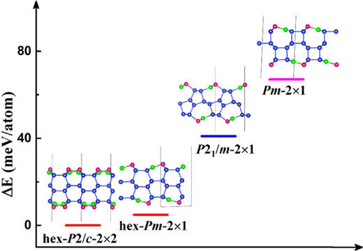 |
| Side views of the lowest-energy and low-lying structures of freestanding tri-layer silicene. The highly protruded Si atoms at the surfaces, the second most protruded Si atoms, and the remaining ones are depicted by magenta, green and blue balls, respectively. The unit cells are indicated by solid lines. The energies are relative to the most stable hex-P2/c-2x2 structure. (© Elsevier) |
| This work is a comprehensive investigation of multilayer silicene. It highlights the most stable multilayer silicene; explores the effect of number of layers and strain on electronic properties; and demonstrates the extra-high photovoltaic efficiency of tri-layer silicene. |
| "By means of ab initio swarm-intelligence structure-searching method, we systemically investigated the low-lying energy structures of freestanding silicene phases from monolayer to penta-layer," Wang explains. "Among them, tri-layer silicene – consisting of alternating arrays of six-membered silicone rings – can be converted into a direct gap semiconductor of 0.86 eV by applying a low tensile strain (∼2.5%). The photovoltaic efficiency of the tri-layer silicene reaches up to 29% at 1.0 µm, which is comparable to that of bulk GaAs with the highest conversion." |
| He adds that the 1 µm-thick tri-layer hex-P2/c- 2x2 silicene could be experimentally engineered by van de Waals stacking. |
| The team used the swarm-intelligence CALYPSO code to search for the energetically most favorable phases of silicene from monolayer to penta-layer. The lowest-energy tri-layer silicene predicted (denoted as hex-P2/c-2x2) consists of alternating arrays of six-membered Si rings. |
| The hex-P2/c-2x2 silicene is semiconducting with a quasi-direct band gap, and is energetically more favorable than the previously reported P21/m-2x1 structure. The indirect-direct band gap transition can occur upon a small external strain in the hex-P2/c-2x2 tri-layer silicene. |
| "Bulk GaAs has the highest conversion efficiency among thin-film solar cell absorbers, and the estimated photovoltaic efficiency of this tri-layer silicene is as high as 29%, comparable to bulk GaAs (32%)," notes Wang. |
| Therefore, the authors believe that the hex-P2/c-2x2 phase holds great potential as ideal candidates for high-efficiency photovoltaic absorbers. |
| To gain a better understanding of structural evolution of multilayer silicene, the research team also computed the electronic properties of multilayer silicene. Interestingly, the odd-layers exhibit quasi-direct characteristics, in contrast, even-layer possess indirect characteristics. |
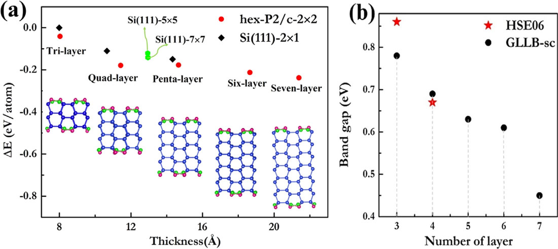 |
| (a) The total energies (in eV/atom) of hex-P2/c-2x2 silicenes with three to seven layers with respect to the previously reported tri-layer P21/m-2x1 (Si (111)-2x1) silicene, the energies for quad-silicenes with Si (111)-5x5 and 7x7 DAS surface reconstructions are given for comparison. (b) The band gaps of the lowest-energy phases of silicenes from tri-layer to seven-layer computed using the GLLB-sc functional, in comparison with the results by HSE06 functional. (© Elsevier) (click on image to enlarge) |
| "Since the PBE functional tend to underestimate band gaps, and the HSE06 functional is very resource intensive, we adopted the GLLB-sc functional to get more accurate band gaps for the multi-layer silicenes." Chen points out. "We found that the band gaps decrease from 0.78 eV to 0.45 eV when increasing the layer number from three to seven, which means that the band gap and its nature can be tuned by controlling the number of layers." |
| "Our study not only identified promising materials for flexible and wearable photovoltaic devices, but also provides a general method to study the geometric structure and electronic property evolution for 2D materials with nonlayered bulk counterparts," he adds. |
| The team will continue to explore promising materials for flexible and wearable photovoltaic devices, and further study on 2D materials with nonlayered bulk counterparts. Efficient computational screening and materials design of experimentally feasible, low-cost, and highly effective low-dimensional materials as absorbers, and their experimentally realization are the key challenges. The scientists note that the interplay and synergy between theory and experiments will greatly facilitate this research area. |
 By
Michael
Berger
– Michael is author of four books by the Royal Society of Chemistry:
Nano-Society: Pushing the Boundaries of Technology (2009),
Nanotechnology: The Future is Tiny (2016),
Nanoengineering: The Skills and Tools Making Technology Invisible (2019), and
Waste not! How Nanotechnologies Can Increase Efficiencies Throughout Society (2025)
Copyright ©
Nanowerk LLC
By
Michael
Berger
– Michael is author of four books by the Royal Society of Chemistry:
Nano-Society: Pushing the Boundaries of Technology (2009),
Nanotechnology: The Future is Tiny (2016),
Nanoengineering: The Skills and Tools Making Technology Invisible (2019), and
Waste not! How Nanotechnologies Can Increase Efficiencies Throughout Society (2025)
Copyright ©
Nanowerk LLC
|

Become a Spotlight guest author! Join our large and growing group of guest contributors. Have you just published a scientific paper or have other exciting developments to share with the nanotechnology community? Here is how to publish on nanowerk.com. |
