| Dec 04, 2018 |
A graphene NEMS switch to protect against electrostatic discharging |
| (Nanowerk Spotlight) One of the most pervasive reliability problems facing the computer chip industry is ESD (electrostatic discharging) failure caused by the rapid, spontaneous transfer of electrostatic charge induced by a high electrostatic field. In order to protect integrated circuits (IC) from being damaged by ESD, chip manufacturers place dedicated ESD protection structures at I/O and power lines on the chip. |
| For decades, conventional on-chip ESD protection structures for ICs has relied on in-Si PN-junction-based device structures (e.g., diodes, bipolar junction transistors, MOSFETs and silicon-controlled rectifiers), which have many inherent disadvantages such as substantial parasitic capacitance, PN junction leakage current, and large Si area consumption, unsuitable for ICs at nanoscale nodes. |
| That's why researchers have been working on novel ESD protection designs for future ICs. However, latent ESD failure mechanisms, accurate ESD device modeling and predictive ESD CAD design verification are some of the challenges that need to be overcome. |
| Recently, a research team led by Professors Albert Wang (University of California at Riverside) and Ya-Hong Xie (University of California at Los Angeles) has devised a novel above-IC graphene based nanoelectromechanical system (NEMS) switch structure (gNEMS) for on-chip ESD protection utilizing the unique properties of graphene. |
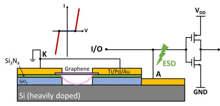 |
| Cross-section and circuit scenario for the new gNEMS switch ESD protection structure. The normal-OFF switch can be turned on by pulling down the graphene membrane by ESD pulses. The inset illustrates an ideal ON-OFF I-V behavior for the gNEMS ESD switch. (© IEEE) |
| As illustrated in the figure above, the gNEMS ESD switch is a two-terminal device with a vacuum gap between a conducting substrate (Si or metal serving as the anode, A) at the bottom and a suspended graphene membrane on top serving as the discharging path. |
| During normal IC operation, the gNEMS switch is at the OFF state and the graphene ribbon is suspended over the trench. When an ESD surge occurs at I/O, the induced electrostatic force pulls down the suspended graphene membrane to touch the bottom conducting layer, forming a discharging path from graphene to ground. |
| "Our novel gNEMS ESD switch can be fabricated in the back end of line (BEOL) fabrication of ICs (where the individual devices such as transistors, capacitors, and resistors get interconnected with wiring on the wafer) through 3D heterogeneous integration, and therefore can eliminate many design problems inherent to traditional in-Si ESD protection structures," Dr. Qi Chen tells Nanowerk. |
| Chen is first author of a paper in IET Micro & Nano Letters ("Systematic transient characterisation of graphene NEMS switch for ESD protection") that provides practical design guidelines for using the gNEMS switch as on-chip ESD protection for ICs. |
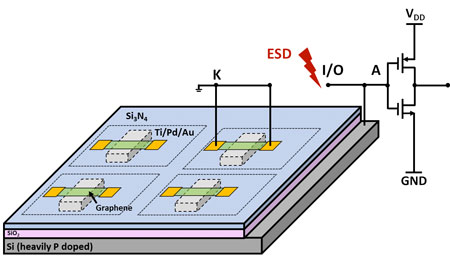 |
| A conceptual illustration for the new gNEMS ESD protection structure and its on-chip ESD protection scenario. (© IEEE) |
| Chen points out that, compared with conventional active ESD devices based on PN junctions, this passive gNEMS switch has several advantages: theoretically, it has zero leakage and minimum parasitic capacitance; it also shows dual-polarity ESD protection features while the conventional counterparts can only work for single-polarity protection, which can largely reduce the ESD device area consumptions. Furthermore, graphene shows superior current and heat handling capability. |
| "Most importantly" he notes, "due to the graphene ESD switch being a passive device, it can be fabricated at the CMOS back end through 3D heterogeneous integration, instead of taking up large chip areas with core IC designs." |
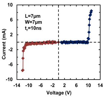 |
| Measured I-V curve by TLP for a prototype gNEMS device shows near symmetric I-V switching behaviors desired for ICs. (© IEEE) |
| The research team developed a CMOS-compatible process to fabricate the graphene NEMS ESD switches. During the fabrication process, graphene is synthesized by chemical vapor deposition (CVD) method instead of micro-exfoliation. |
| According to the team, the CVD method also provides a promising route for graphene ESD switch mass production. |
| "We also conducted systematic transient characterization of our gNEMS ESD switches by transmission line pulse (TLP) measurement for human body model ESD protection, revealing transient ESD discharging behaviors related to device dimensions and TLP pulse shapes," says Chen. "The results provide practical design guidelines for using graphene ESD switches as on-chip ESD protection for ICs." |
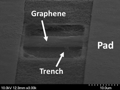 |
| SEM image of a gNEMS ESD switch showing the suspended graphene membrane over a trench. (© IEEE) |
| Going forward, the team will try to fabricate the graphene ESD switch by 3D heterogenous integration at the IC backed with foundry processed chips for real applications. Furthermore, they are planning to improve the switches' ESD performance by designing novel NEMS structures and improving the quality of the used graphene material. |
| "While graphene's unique properties – atomic layer thickness, electron mobility, thermal conductivity, mechanical strength – make it an ideal material for ESD protection, the main challenge is the quality of the graphene material," Chen concludes. "Currently, due to graphene quality issues during CVD synthesis, reliability and uniformity is a major challenge for the mass production and real application of graphene for ESD applications." |
 By
Michael
Berger
– Michael is author of four books by the Royal Society of Chemistry:
Nano-Society: Pushing the Boundaries of Technology (2009),
Nanotechnology: The Future is Tiny (2016),
Nanoengineering: The Skills and Tools Making Technology Invisible (2019), and
Waste not! How Nanotechnologies Can Increase Efficiencies Throughout Society (2025)
Copyright ©
Nanowerk LLC
By
Michael
Berger
– Michael is author of four books by the Royal Society of Chemistry:
Nano-Society: Pushing the Boundaries of Technology (2009),
Nanotechnology: The Future is Tiny (2016),
Nanoengineering: The Skills and Tools Making Technology Invisible (2019), and
Waste not! How Nanotechnologies Can Increase Efficiencies Throughout Society (2025)
Copyright ©
Nanowerk LLC
|

Become a Spotlight guest author! Join our large and growing group of guest contributors. Have you just published a scientific paper or have other exciting developments to share with the nanotechnology community? Here is how to publish on nanowerk.com. |
