| Mar 25, 2019 |
Graphene transfer using an off-the-shelf office laminator |
| (Nanowerk Spotlight) One of the most common ways of producing high-quality graphene in sizeable quantities is by chemical vapor deposition (CVD) of methane gas onto a metallic substrate, usually copper. In order for the graphene then to be used in its intended application, it needs to be transferred from the growth substrate to a target substrate – a challenging but extremely important process step. This is typically done by spin-coating a supporting polymer layer and then chemically dissolving away the copper to release the graphene film from the substrate. |
| Although CVD is an industrially scalable process, the transferred graphene produced in this way is prone to contamination from the chemical agents used to remove the growth substrate as well as ripping and tearing. Electrochemical and dry delamination of CVD-grown graphene have been demonstrated, but the material still suffers from some processing-related contamination. |
| "After the growth process, the graphene is firmly attached to a copper foil and while it may well be the world's strongest material, it requires almost nothing to tear or contaminate the graphene," says Peter Bøggild, a professor at Technical University of Denmark (DTU). "So it's hard! If you do an image search on 'graphene transfer' in Google, it is obvious that researchers have tried hundreds of complicated recipes to solve this problem." |
| "Imagine moving a piece of kitchen film from one surface to another, without it becoming curled or dirty," he continues. "It's almost impossible. Then imagine doing the same with graphene, which is 25,000 times thinner (kitchen film about 10 µm, graphene 0.0003 µm). In 2009, the enthusiasm for discovering how easily the graphene could be grown on copper foil was quickly replaced by the question: How do we move it to where we are going to use it?" |
| In new work published in Chemistry of Materials ("Do-it-yourself transfer of large-area graphene using an office laminator and water"), the team of researchers from Denmark, China and Korea, demonstrate a simple method for transferring A4-size sheets of CVD graphene from copper foils onto a target substrate using a commercially available polyvinyl alcohol (PVA) polymer foil as a carrier substrate and an off-the-shelf office laminator. |
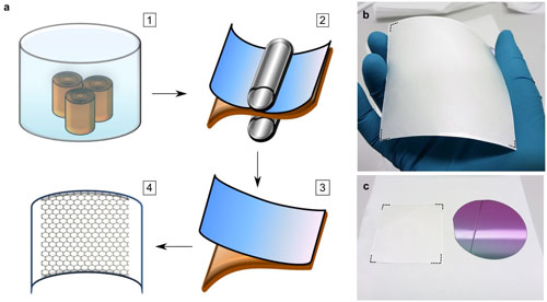 |
| (a) Schematic illustration of the PVA lamination transfer process of graphene: (1) copper foils with as-grown graphene are oxidized in DI water at room temperature for more than 8 hours (overnight); (2) the oxidized foils are subsequently laminated with a commercially available PVA film using a commercial hot-roll laminator. (3) After a 30 second bake on a hot plate at 110°C, the PVA film is mechanically delaminated from the copper surface, taking the graphene film along with it (4). (b-c) Graphene transferred from a 10 cm x 10 cm copper foil; the dashed lines serve as a visual guide marking the edges of the graphene sheet on PVA film. (c) PVA-graphene film (from panel (b)) compared to a 4" SiO2 on Si wafer. (Reprinted with permission by American Chemical Society) |
| This do-it-yourself approach requires few tools and low cost materials – it is safe and easy enough to be carried out in school physics classes. There are no chemicals involved besides water; no spinner; no dangerous etchants. |
| "PVA is widely used in industry already. It’s non-toxic, biodegradable and can be washed away using only water," says Tim Booth, the Associate Professor at DTU who led the work. "It’s an ideal material to base an industrial process on." |
| "We can transfer monolayer graphene from copper foils using a cheap office laminator in just a few minutes," explains Abhay Shivayogimath, the paper's first author. "It is fast and easy. The best part is that we show that this method beats the two most common existing transfer methods by lengths. It is a process that anyone can learn in 20 minutes, with an equipment cost of no more than a few hundred dollars." |
| The inventor Abhay Shivayogimath from the Center for Nanostructured Graphene at DTU Physics, shows how to do it. |
| The team's invention could be quite exciting for graphene producers. Now they can supply graphene in bulk on water soluble backing foil that customers can laminate onto their desired substrate. The customers don’t need any special experience, equipment or chemicals to complete the transfer. |
| The researchers note that this process can also be used to transfer other 2D materials, not just graphene, from metal surfaces. |
| But how about the quality? According to the team, this DIY method beats the other two dominant methods: chemical etching and bubbling transfer. Because only water is used in the whole process, there is virtually no contamination left on the graphene. |
| "In our paper we show that graphene transferred via PVA lamination has lower and more homogeneous residual doping, higher charge carrier mobility, and fewer transfer-induced defects as compared to standard chemical etching or electrochemical delamination transfers," Shivayogimath concludes. "By avoiding any complex processing, the need for catalyst etching and recovery and the use of organic solvents; and using only nontoxic and biodegradable materials, we have demonstrated a process which is greener, lower cost, highly scalable and more convenient for graphene growers and end-users than existing techniques, and has considerable potential for further development and use in research and industry." |
 By
Michael
Berger
– Michael is author of four books by the Royal Society of Chemistry:
Nano-Society: Pushing the Boundaries of Technology (2009),
Nanotechnology: The Future is Tiny (2016),
Nanoengineering: The Skills and Tools Making Technology Invisible (2019), and
Waste not! How Nanotechnologies Can Increase Efficiencies Throughout Society (2025)
Copyright ©
Nanowerk LLC
By
Michael
Berger
– Michael is author of four books by the Royal Society of Chemistry:
Nano-Society: Pushing the Boundaries of Technology (2009),
Nanotechnology: The Future is Tiny (2016),
Nanoengineering: The Skills and Tools Making Technology Invisible (2019), and
Waste not! How Nanotechnologies Can Increase Efficiencies Throughout Society (2025)
Copyright ©
Nanowerk LLC
|

Become a Spotlight guest author! Join our large and growing group of guest contributors. Have you just published a scientific paper or have other exciting developments to share with the nanotechnology community? Here is how to publish on nanowerk.com. |
