| Apr 24, 2019 |
Perfectly-absorbing photoconductive metasurface significantly improves THz detection |
| (Nanowerk Spotlight) Terahertz (THz) radiation is a very safe type of radiation due to its low-energy photons, with more than a hundred times less energy than that of photons in the visible light range. This means that THz imaging could, in some applications, replace x-rays, which are much more damaging to materials and organic tissue. But precisely because it has low energy, THz radiation is challenging to detect. |
| Already THz technology is becoming a key element in applications such as security (such as airport scanners), wireless data communication, medical diagnostics, astronomy, and quality control |
| Terahertz frequencies, which occupy a middle ground between microwaves and infrared light, are seen as the future of wireless communications because they offer a higher bandwidth capacity for data transmission than currently used microwave radiation. |
| A key technology for existing photonic devices operating in the THz frequency range is an ultrafast photoconductive (PC) switch, an optoelectronic element, which changes electrical conductivity under illumination between a highly resistive (OFF) and highly conductive (ON) state within a subpicosecond time period. |
| "The PC switch performance relies on the following three essential requirements: 1) a subpicosecond recombination time for photoexcited charge carriers; 2) a high contrast in conductivity for the ON and OFF states; and 3) an efficient conversion of photons to charge carriers," Dr. Oleg Mitrofanov from the University College London (UCL), explains to Nanowerk. "To produce an efficient PC switch, all three requirements must be met simultaneously." |
| Addressing these challenges, Mitrofanov and his collaborators from UCL and Sandia National Laboratories have developed a perfectly-absorbing photoconductive metasurface, which can be switched between an electrically insulating state to a highly conductive state with light of specified wavelength. |
| This perfect absorption without the incorporation of any metallic structures or back reflectors is enabled by nanostructures supporting two resonant modes of opposite symmetry – odd and even with respect to the metasurface plane – provided that the two modes are degenerate and critically coupled. |
| This metasurface – a very thin layer of carefully nanostructured material – is practically invisible when it is placed onto glass. The perfect absorption within this metasurface allows to make the active region of THz wave detectors significantly thinner in comparison to conventional detectors. Apart from reducing the size of THz detectors, it also improves their efficiency. |
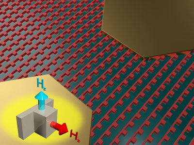 |
| Conceptual illustration of the perfectly absorbing photoconductive metasurface comprising a network of resonators with broken symmetry and integrated into a THz detector. The inset at the bottom left illustrates schematically two resonant modes (magnetic dipoles Hx and Hz ) supported by the resonators. (Image modified and partially reprinted with permission from American Chemical Society) |
| The team has reported their findings in Nano Letters ("Terahertz Detection with Perfectly-Absorbing Photoconductive Metasurface"). |
| To demonstrate the practical applicability of their design, the researchers integrated this metasurface into photoconductive THz detectors and achieved THz pulse detection with signal-to-noise ratio of more than 6 orders of magnitude using an unprecedentedly low level of ultrafast laser excitation of 100 µW. |
| "Our work has direct implications for THz photoconductive detectors, which can be made smaller and would require optical power about ten times less than the conventional detectors," Mitrofanov points out. "We also anticipate that functionality achieved with this photoconductive network can be applied for other applications, for example efficient modulators and THz emitters." |
| The scientists are also interested in integrating these photoconductive metasurfaces into practical THz devices, for example in THz near-field microscopy probes, which enable THz imaging and spectroscopy with spatial resolution much better than the diffraction limit. |
| Mitrofanov adds that the concept of photoconductive metasurface, where not only optical but also electronic properties are engineered, introduces another dimension for metasurface research, which he anticipates will find several practical applications. |
 By
Michael
Berger
– Michael is author of four books by the Royal Society of Chemistry:
Nano-Society: Pushing the Boundaries of Technology (2009),
Nanotechnology: The Future is Tiny (2016),
Nanoengineering: The Skills and Tools Making Technology Invisible (2019), and
Waste not! How Nanotechnologies Can Increase Efficiencies Throughout Society (2025)
Copyright ©
Nanowerk LLC
By
Michael
Berger
– Michael is author of four books by the Royal Society of Chemistry:
Nano-Society: Pushing the Boundaries of Technology (2009),
Nanotechnology: The Future is Tiny (2016),
Nanoengineering: The Skills and Tools Making Technology Invisible (2019), and
Waste not! How Nanotechnologies Can Increase Efficiencies Throughout Society (2025)
Copyright ©
Nanowerk LLC
|

Become a Spotlight guest author! Join our large and growing group of guest contributors. Have you just published a scientific paper or have other exciting developments to share with the nanotechnology community? Here is how to publish on nanowerk.com. |
