| Aug 22, 2019 |
Atomically thin straintronic devices |
| (Nanowerk Spotlight) Strain engineering is a general strategy employed in semiconductor manufacturing to enhance device performance. The goal is to tune the bandgap of a semiconductor by the application of strain. Strain engineering also has emerged as an interesting way to control the electrical and optical properties of two-dimensional (2D) materials. |
| For instance, researchers have discovered that local strain in a graphene sheet can alter its conducting properties. By varying the amount of local strain, transport gaps can be tailored (read more: "Strain engineering graphene's transport"). |
| By studying flexible and transparent photodetectors based on single-layer MoS2 under the application of biaxial strain, researchers at the Consejo Superior de Investigaciones Científicas (CSIC, the Spanish National Research Council) have developed atomically thin photodetectors whose characteristics can be controlled by means of an externally applied strain. This strain can be reversibly applied through the thermal expansion (shrinkage) of the substrate material, which induces tensile (compressive) biaxial stress. |
| These results, published in the journal Materials Today ("A strain tunable single-layer MoS2 photodetector"), emphasize the possibilities of a new kind of electronics – straintronics – in which mechanical deformations are used to modify not only the geometry of the device, but its properties and performance as well. |
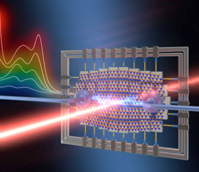 |
| Artistic representation of the MoS2 photodetector device while subjected to biaxial strain. (Image: E. Sahagún, Scixel) |
| "By stretching the MoS2 photodetectors, we can increase their bandwidth and responsitivity, although the device would become slower," explains Andres Castellanos-Gomez, CSIC researcher in the Instituto de Ciencia de Materiales de Madrid. "In the same way, if we compress the photodetectors, we observe a noticeable decrease in the response time but they present a smaller bandwidth and responsitivity." |
| "In our study, we found that by controlling the level of strain, we can tune the photoresponsitivity by 2–3 orders of magnitude, the response time from less than 80 ms to 1.5 seconds, and the spectral bandwidth with a gauge factor of 135 meV/% or 58 nm/% of the device," he adds. |
| Fast strain-tuning the optoelectronic performance of photodetector devices opens up the possibility to fabricate artificial photonic devices that mimic the adaptability of the human eye to different light conditions. |
| "For example, this technology could have future applications in the photography field, in the change from day/night modes depending on the light intensity," says Patricia Gant, first author of the paper. "The camera detector would change the response to adjust the performance according to the light through a small deformation controlled by the user." |
| "Our work demonstrates that 2D semiconductors hold a great promise for future straintronic devices where strain is employed as a variable tuning knob," Castellanos-Gomez concludes. |
| He points out that the method to strain-tune the band structure presented in this paper is general and can be applied to photodetectors based on other 2D materials. |
 By
Michael
Berger
– Michael is author of four books by the Royal Society of Chemistry:
Nano-Society: Pushing the Boundaries of Technology (2009),
Nanotechnology: The Future is Tiny (2016),
Nanoengineering: The Skills and Tools Making Technology Invisible (2019), and
Waste not! How Nanotechnologies Can Increase Efficiencies Throughout Society (2025)
Copyright ©
Nanowerk LLC
By
Michael
Berger
– Michael is author of four books by the Royal Society of Chemistry:
Nano-Society: Pushing the Boundaries of Technology (2009),
Nanotechnology: The Future is Tiny (2016),
Nanoengineering: The Skills and Tools Making Technology Invisible (2019), and
Waste not! How Nanotechnologies Can Increase Efficiencies Throughout Society (2025)
Copyright ©
Nanowerk LLC
|

Become a Spotlight guest author! Join our large and growing group of guest contributors. Have you just published a scientific paper or have other exciting developments to share with the nanotechnology community? Here is how to publish on nanowerk.com. |
