| Oct 21, 2020 |
Kelvin probe force microscopy - what is it? How does it work? |
| (Nanowerk Spotlight – Application Note) Kelvin probe force microscopy (KPFM), also known as surface potential microscopy, is one member of a suite of electrical characterization methods available in atomic force microscopes. It maps the contact potential difference (CPD) between a surface and the cantilever, containing information about the surface potential and work function. |
| The work-function is defined in solid-state physics as the energy needed to remove an electron from the Fermi level of a solid to the vacuum and is thus, a surface property and not related to the bulk. |
| KPFM is a surface-sensitive method that probes at and near the surface only. It is often used as a qualitative technique to obtain contrast based on the surface potential. |
| Quantitative scanning Kelvin probe force microscope measurements of the local work function are generally performed in vacuum and require a model to describe the electrostatic interactions between the tip and sample as well as knowing the work function of the tip. |
| In ambient conditions, the contact potential difference is influenced by surface contaminations of tip and sample as well as surface water films, which additionally hampers the calculation of the work function of a sample surface from the CPD. |
How does it work? |
| On Nanosurf AFMs, Kelvin probe force microscopy operates in dynamic force mode where a cantilever with a thin electrically conductive coating is driven near its resonance frequency. Soft dynamic mode cantilevers coated with platinum-iridium (PtIr) are suitable for most KPFM experiments and are not much more expensive than their non-conductive variants. Alternatively, cantilevers coated with conductive diamond-like carbon or Platinum silicide are available and are more wear resistant compared to PtIr. |
| An AC voltage, with frequency far away from the resonance frequency, is applied to the cantilever to measure the CPD between the surface and the cantilever. This creates an oscillating electrostatic force between the tip and sample that is measured by a second internal lock-in amplifier in the controller (Figure 1). |
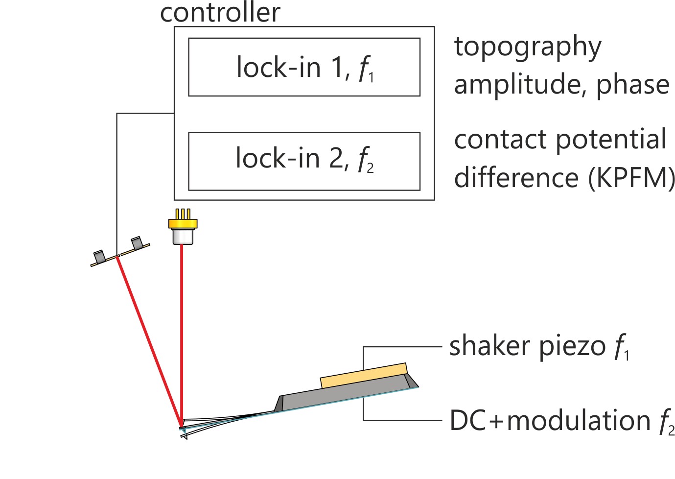 |
| Figure 1. Schematic of KPFM. (Image: Nanosurf) |
| A DC offset voltage is then added to the AC voltage to cancel out the cantilever oscillation at the AC frequency. By recording the applied DC offset voltage while the tip is scanned across the surface, a representation of the CPD emerges. An easy to use KPFM routine in the Nanosurf software makes setting up KPFM measurements straight forward, thereby enabling even novice users to collect KPFM data. |
| KPFM can operate in either a single or dual-pass mode. In single-pass mode, the cantilever passes over every line once while simultaneously recording topography and CPD. |
| The advantage of single-pass mode is that the simultaneous recording of the topography and CPD improves correlation between the signals. If the amplitude of cantilever oscillation is kept small, the tip is close to the surface, which results in higher sensitivity and resolution of the KPFM measurement. Single pass KPFM is faster and minimizes tip wear but is more prone to artifacts at edges and boundaries. |
| In the dual-pass setup, the cantilever passes twice over every line in the image. During the first pass, the topography information is collected. The tip is then offset or lifted above the sample during the second pass by a user-determined distance, typically a few tens of nanometers. The CPD as described above is recorded. |
| Dual-dual pass measurements are inherently slower than single-pass measurements because every line must be imaged twice. Preferably the topography as recorded during the first pass is used during the second pass to obtain constant tip-sample separation. While requiring longer acquisition time than the single-pass method, the benefit is less edge and boundary artifacts and less nosier images. By reducing the oscillation of the cantilever during the second pass, the lift height can be reduced, thus improving the KPFM contrast. |
KPFM Applications |
| A. Multilayer Graphene: Multilayer graphene can exhibit interesting electrical properties depending on its composition. An 8 x 8 µm image at the edge of a graphene flake is shown in Figure 2. |
| The sample is a multilayer graphene flake generated by mechanical exfoliation of graphite and subsequently transferred to a silicon-silicon dioxide substrate. The left image is the topographical map while the bottom image shows the KPFM signal overlaid on a 3D representation of the surface topography. The color contrast in this map represents the KPFM signal or the contact potential difference. Areas that are colored purple or pink represent areas with high contact potential difference while areas that are colored green have low contact potential difference. |
| Through this CPD map, the electrical properties at different thicknesses of the flake is evident as the thin flakes on top have high contact potential (blue) while the rest of the layer has a lower contact potential (green). |
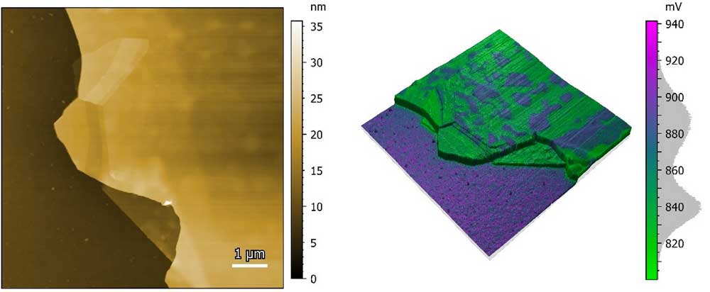 |
| Figure 2. Multilayer graphene. The left image is an 8 x 8 µm topography image while the right image shows the 3D representation of the surface topography overlaid with the contact potential difference. (Sample courtesy of Hiske Overweg and Klaus Ensslin, ETH Z?rich, Switzerland) (click on image to enlarge) |
| B. MoS2 Monolayer: An example of the power of KPFM, especially as a method to provide electrical properties contrast is shown in the study of a molybdenum disulfide (MoS2) monolayer, which was grown by chemical vapor deposition (CVD). Using a Flex-Axiom, KPFM reveals the contact potential difference variations within a single crystal as well as variations between the single crystal and the underlying SiO2 substrate. |
| An 18 x 18 µm image of the monolayer is shown in figure 3. The left image is the topography while the right image shows the KPFM signal overlaid on a 3D representation of the surface topography. The monolayer is only 0.6 nm thick yet there is a 650 mV contact potential difference between the monolayer and the substrate. The contact potential signal varies across the monolayer, providing information regarding doping profiles and other surface defects. |
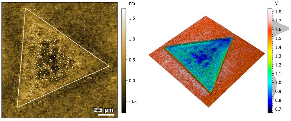 |
| Figure 3. MoS2 Monolayer. The left image is an 18 x 18 µm topography image while the right image shows the 3D representation of the surface topography overlaid with KPFM signal. (click on image to enlarge) |
| C. KPFM on Steel: Stainless steel is a metal alloy composed from elements such as chromium, aluminium and carbon and held together in a ferrite matrix. The work potential of each of the elements that make up the steel will be slightly different, thus KPFM can be used to show how each composite is distributed across the alloy. An 80 x 80 µm image of polished and electrochemically etched stainless steel is shown in figure 4. |
| The left image is the topography while the right image shows the single-pass KPFM signal. The topography image shows that polishing the steel resulted in a very smooth surface (RMS roughness = 3.9 nm) over the 80 µm image. The KPFM image shows a difference of 80 mV between the inclusions (blue) and the ferrite (green/yellow) matrix. The yellow streak across the bottom of the KPFM image was caused by a modification to the tip from the defect visible at the bottom left of the topography image. |
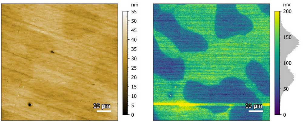 |
| Figure 4. Stainless Steel. The left image is an 80 x 80 µm topography image while right image shows the KPFM signal collected simultaneously. (click on image to enlarge) |
| D. Insulating Oxide surface: An example using dual-pass KPFM to image an insulating oxide is shown in Figure 5. In this sample, charges were locally deposited in an insulating oxide surface layer in a Swiss-cross pattern. The left image is a 10 x 10 µm topography image, which shows no indication of any Swiss-cross pattern but the KPFM image on the right clearly reveals the location of the buried charges within the insulating oxide surface. |
 |
| Figure 5. KPFM of locally deposited charges on an insulating oxide surface. The left image shows the surface topography while the right image is the KPFM image. (Image courtesy of Marcin Kisiel, Thilo Glatzel and students of the Nanocurriculum of the University of Basel, Switzerland) (click on image to enlarge) |
KPFM as improvement tool for other modes |
| During dynamic mode imaging, the contact potential difference between the tip and a sample influences the cantilever oscillation. This implies that topography measurements in heterogeneous samples in dynamic mode are affected by contact potential variations of the sample and needs to be compensated. |
| In other words, the measured height difference between two dissimilar materials contains an error caused by the CPD heterogeneity of the materials. Using KPFM feedback during topographical measurements can compensate for this error thereby enhancing the accuracy of AFM measurements on heterogeneous materials. |
| The same can be said for MFM measurements. In MFM, the phase close to the resonance frequency of the cantilever is used to measure the force resulting from local magnetic dipole moments. However, the phase does not distinguish magnetic forces from electrostatic forces. Applying KPFM during MFM measurements will reduce the effect of electrostatic forces on the phase shift, increasing the accuracy of the MFM data. |
| Provided by Nanosurf AG |

Become a Spotlight guest author! Join our large and growing group of guest contributors. Have you just published a scientific paper or have other exciting developments to share with the nanotechnology community? Here is how to publish on nanowerk.com. |
