| Oct 27, 2020 |
Solar-powered smart dust |
| (Nanowerk Spotlight) Some 20-30 years ago, microelectromechanical systems (MEMS) emerged in industrial manufacturing in a major way. MEMS consist of any combination of mechanical (levers, springs, membranes, etc.) and electrical (resistors, capacitors, inductors, etc.) components to work as sensors or actuators. |
| The size of today's smartphones would be impossible without the use of numerous MEMS devices. Apart from accelerometers and gyroscopes, smartphones contain micro-mirrors, image sensors, auto-focus actuators, pressure sensors, magnetometers, microphones, proximity sensors and many more. Another example from everyday life is the use of MEMS as accelerometers in modern automobile airbags where they sense rapid deceleration and, if the force is beyond a programmed threshold, initiate the inflation of the airbag. |
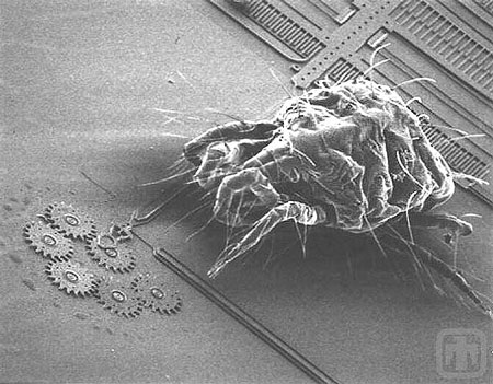 |
| A mite, less than 1 mm in size, approaching a microscale gear chain. (Image: Sandia National Laboratories) |
What is Smart Dust? |
| Industrial ubiquity of MEMS, increasing computing power of chips, the miniaturization of lab-on-a-chip devices, and increased connectivity, combined with the emergence of nanotechnologies, gave rise to the concept of smart dust – sub-millimeter-scale autonomous computing and sensing platforms not larger than a grain of sand. |
| An individual smart dust particle in itself is a tiny sensor and computer, self-powered and wirelessly connected to a large network. Each particle can be left unattended and collects environmental data such as light, temperature, pressure, vibrations, the existence of toxins etc. and transmits this data wirelessly to larger, remote computer systems – or, depending on the available computing power, processes it directly at the point of data collection. |
| A large number of these particles dispersed over an area would be left to interact with their environment and then communicate their findings to a host where the collected data is processed and analyzed. |
| Smart dust particles are the ultimate Internet-of-Things (IoT) devices. They are revolutionary because the sensors are small enough to be put anywhere and work wirelessly, sharing data. Smart dust will lead to ubiquitous autonomous artificial intelligent computation near the end user, such as authentication, medical procedures and health care monitoring, sensing and tracking, industrial and supply chain monitoring, and defense applications. |
Smart Dust Concepts |
| For instance, DARPA's SHIELD program plans to use microscale chips to track and authenticate the supply chain of IC chips for defense applications. The goal is to eliminate counterfeit integrated circuits from the electronics supply chain by making counterfeiting too complex and time-consuming to be cost effective. SHIELD aims to combine NSA-level encryption, sensors, near-field power and communications into a tiny chip capable of being inserted into the packaging of an integrated circuit. |
| More advanced concepts even envision programmable smart dust that triggers an automatic response, for instance the triggering of an alarm signal when invisible microcracks are detected in a turbine blade. |
| Smart dust is a concept that has been proposed some 20 years ago. However, the main challenges researchers have been grappling with are the lack of enough power on the small footprint and the difficulties of integrating power systems into these highly scaled devices. Since the storage density of battery technologies has not followed Moore's law scaling trends, IoT systems need to rely on power conversion from outside sources such as thermal, vibrational, light, or radio waves. |
| "As nanoelectronics and packaging technologies evolve, though, now may be the right time that we start to rethink the solutions for these problems and advance towards more powerful small computer systems than what was originally proposed," says Dr. Ning Li, a researcher at IBM's T J Watson Research Center in Yorktown Heights, NY. |
Advances in Nanoelectronics Reduce the Footprint of Smart Dust |
| Recent advancements in nanoelectronics are well suited to enable these autonomous edge computing platforms with a very small, i.e. micrometer-scale, footprint ('edge computing' is a term to describe a distributed computing framework that brings enterprise applications closer to data sources such as IoT devices). However, power source and communication devices still remain the key bottle neck, due to their difficulty to scale down sufficiently and the lack of a straightforward integration process. |
| And although tiny computing systems have a low cost because the number of chips per wafer is very large, their packaging cost is extremely high, making the large-scale use of these devices cost-prohibitive. |
| In a new paper in Advanced Materials ("Dust-Sized High-Power-Density Photovoltaic Cells on Si and SOI Substrates for Wafer-Level-Packaged Small Edge Computers"), a team of scientists at IBM demonstrates that dust-sized photovoltaic cells grown on silicon substrate can be heterogeneously integrated with other chiplets – integrated circuit blocks that has been specifically designed to work with other similar chiplets to form larger more complex chips – using a high-throughput wafer-level packaging process. |
Nanoelectronic Chiplets |
| The ability to integrate various nanoelectronic chiplets – such as processor, memory, and photovoltaics – in an industrial-scale wafer-level-packaging process, unlocks the potential of large-scale manufacturing of these compact integrated systems with high performance and ultralow cost. |
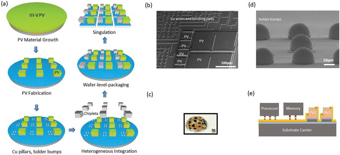 |
| Wafer-level high-throughput processing of small footprint edge computers: a) Schematics illustrating processing steps including: III-V PV growth on SOI substrate, a PV mesa etched down to the buried oxide layer, PV cell fabrication and copper (Cu) interconnect, Cu pillar and solder bump formation for chip packaging, wafer level selective bonding of fabricated chips, including microprocessor, nonvolatile memory, sensors, etc., and chip singulation using deep Si reactive ion etching. b) Scanning electron microscopy image of SOI wafer carrier with integrated PV after fabrication with Cu wire and pads for Cu pillar and solder bumps. c) A picture of the finished device taken together with a ladybug to illustrate its size. d) Scanning electron microscopy image of solder bumps. e) Cross-section schematic illustrating a packaged small computer system. (Reprinted with permission by Wiley-VCH Verlag) |
| As illustrated in the figure above, the researchers first grow photovoltaic materials on an SOI substrate, and then etched them into mesa structures all the way down to the buried oxide layer. The photovoltaics are fabricated with electroplated copper (Cu) interconnect for series connection. The Cu pillars and solder bumps are then fabricated on bonding pads, connected by the Cu bonding pads. Then, the team bonded separately fabricated processor and memory chips onto the SOI carrier wafer in a wafer-level-packaging process. They used deep reactive-ion-etching for singulation with very low kerf loss. |
| A double benefit of the small size and thin layers of the photovoltaic cells on the chips is the simultaneous conversion of power and the reception of high-speed optical signals. |
| "We were able to show that the negative effect of material defects in the heteroepitaxial growth of III-V PV on Si becomes less significant as power density increases, favoring the approach of using directly grown III-V materials on Si substrate as integrated micro-PV at high power density," the IBM team explains. "Our III-V photovoltaics grown on Si shows multiple times higher efficiency and an order of magnitude higher output power density than prior Si micro-PVs due to better charge collection at high illumination intensity using III-V material grown on Si." |
| The team's approach to make these III-V PVs on Si currently is the only approach that allows the utilization of wafer-level-packaging to integrate other chiplets. This is a big advancement over all prior processes that use pick-and-place and wire bonding to integrate chiplets. |
| "Our high-throughput wafer-level-packaging process, enabled by the monolithically integrated III-V micro-PV on Si, unlocks the long-expected potential of low-cost and high-throughput manufacturing of these small computers especially for large-scale IoT applications," the researchers conclude. |
 By
Michael
Berger
– Michael is author of four books by the Royal Society of Chemistry:
Nano-Society: Pushing the Boundaries of Technology (2009),
Nanotechnology: The Future is Tiny (2016),
Nanoengineering: The Skills and Tools Making Technology Invisible (2019), and
Waste not! How Nanotechnologies Can Increase Efficiencies Throughout Society (2025)
Copyright ©
Nanowerk LLC
By
Michael
Berger
– Michael is author of four books by the Royal Society of Chemistry:
Nano-Society: Pushing the Boundaries of Technology (2009),
Nanotechnology: The Future is Tiny (2016),
Nanoengineering: The Skills and Tools Making Technology Invisible (2019), and
Waste not! How Nanotechnologies Can Increase Efficiencies Throughout Society (2025)
Copyright ©
Nanowerk LLC
|

Become a Spotlight guest author! Join our large and growing group of guest contributors. Have you just published a scientific paper or have other exciting developments to share with the nanotechnology community? Here is how to publish on nanowerk.com. |
