| Jan 27, 2021 |
A brief history of OLEDs |
| (Nanowerk Spotlight) Eastman Kodak's Research Laboratories have been a ground-breaking pioneer in developing organic light-emitting diode (OLED) technology. In the 1970s, the company's scientists developed the first viable OLED material and in 1987, Kodak researchers demonstrated the first OLED device operated at sufficiently low voltages to allow for commercial applications (Applied Physics Letters, "Organic electroluminescent diodes"). |
| OLED technology is based on the phenomenon that certain organic materials emit light when fed by an electric current. OLED technologies makes it possible to manufacture ultra flat, very bright and power-saving OLED televisions, windows that could be used as light source at night, and large-scale organic solar cells. |
| In contrast to a regular light-emitting diode (LED), the emissive electroluminescent layer of an OLED consists of a thin-film of organic compounds. What makes OLEDs so attractive is that they do not require a backlight to function and therefore require less power to operate; also, since they are thinner than comparable LEDs, they can be printed onto almost any substrate. |
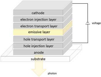 |
| OLEDs are typically thin multilayer devices that consist of layers of organic semiconductors. Schematic depiction of a stacked device structure of an OLED. (Reprinted with permission by Wiley-VCH Verlag) |
| Moreover, OLED displays show improvements in resolution, wider viewing angles, high contrast colors, faster response time, and the possibility to realize transparent displays. Another major benefit is the realization of flexible OLED displays that can be bent and rolled up like a poster, which opens a new dimension to the design possibilities of large-scale flexible displays. |
| This is the basic process behind the light-generation in OLEDs: The charge carriers – electrons and holes – are obtained at the cathode and anode, respectively, by applying an external voltage. Subsequently, the charge carriers are injected into the electron and hole injection layers. Next, the electrons and holes migrate through the electron and hole transport layers into the emissive layer, where the recombination of the charge carriers and the formation of excitons (the bound states of an electron and an electron hole) takes place. The electroluminescence, i.e. the emittance of visible light, occurs as these excitons relax radiatively from the excited state to the ground state. |
| Although more than 14 000 journal publications, 13 000 patents, over 1 000 reviews, and several books have been released over the past decades, a very informative review article in Advanced Materials ("A Brief History of OLEDs – Emitter Development and Industry Milestones") summarizes the historic development of OLEDs in industry and the OLED emitters in academia. |
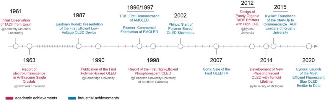 |
| Overview of milestones in OLED technology; PMOLED–passive matrix OLED, AMOLED–active matrix OLED. (Reprinted with permission by Wiley-VCH Verlag) (click on image to enlarge) |
| The review focuses on three main topics: 1) a curated historic perspective on the emitter development on the side of academia, which includes metal-based and purely organic emitters built into green, orange-red and blue OLED devices; 2) selected information on the OLED development over the past three decades on the side of the industry; and 3) a perspective on the next up-coming “fourth generation” of light-emitting materials for OLEDs. |
| For OLED devices, the generated singlet excitons and triplet excitons are in a 25% to 75% ratio. To obtain satisfying device performances with high external quantum efficiencies, the development and design of light-emitting materials for OLEDs, which have the potential to fully harvest the singlet excitons and triplet excitons, are of utmost importance. |
| As the authors discuss in great detail in the main section of their review, three generations of emitters have been elaborately studied and developed to realize this goal and the next generation of emitters is currently being developed in parallel. |
| The first three generations are subdivided into green, orange-red, and blue emitters as green OLED emitters were introduced before red, and red before blue. These three red, green, and blue colors are crucial for the color saturation of OLED devices. |
| Please note that the authors deliberately excluded discussion of the development of device structure, host materials, and other components of OLEDs. Moreover, emitters that are exclusively reported in patents, white OLEDs, and OLEDs with emitters based on polymers are not covered within the scope of this report. |
| Next-generation emitting materials are fast-emerging and, as the authors note, the history of OLED development has yet another season of even better devices coming. Concluding their review, the authors highlight two promising approaches to innovating OLED technology. |
| One strategy to further improve the light-output of OLED devices is the usage of well-ordered structures like (surface-mounted) metal-organic frameworks (SUR)MOFs to tune the electron-hole mobility. Consequently, SURMOFs should be considered for future stack architectures of OLED devices. |
| A different approach to innovation uses luminophores that intrinsically emit circularly polarized light to achieve higher brightness of OLEDs, and a simplified and thinner OLED device architecture. Luminophores enable high light yields and would be inexpensive to produce on a large scale. Researchers have been searching for such materials for a long time. The newly generated understanding will facilitate the rapid and cost-efficient development of new lighting appliances in the future. |
 By
Michael
Berger
– Michael is author of four books by the Royal Society of Chemistry:
Nano-Society: Pushing the Boundaries of Technology (2009),
Nanotechnology: The Future is Tiny (2016),
Nanoengineering: The Skills and Tools Making Technology Invisible (2019), and
Waste not! How Nanotechnologies Can Increase Efficiencies Throughout Society (2025)
Copyright ©
Nanowerk LLC
By
Michael
Berger
– Michael is author of four books by the Royal Society of Chemistry:
Nano-Society: Pushing the Boundaries of Technology (2009),
Nanotechnology: The Future is Tiny (2016),
Nanoengineering: The Skills and Tools Making Technology Invisible (2019), and
Waste not! How Nanotechnologies Can Increase Efficiencies Throughout Society (2025)
Copyright ©
Nanowerk LLC
|

Become a Spotlight guest author! Join our large and growing group of guest contributors. Have you just published a scientific paper or have other exciting developments to share with the nanotechnology community? Here is how to publish on nanowerk.com. |
