| Oct 28, 2021 |
Calligraphy at the nanoscale |
| (Nanowerk Spotlight) Nanotechnology device fabrication – from electronics to photonics, security, biotechnology and medicine – often requires some form of nanopatterning technique in order to achieve the structures and surfaces required for the device. And although they may not be visible to the naked eye, the nanometer-sized trenches, ridges, curves and grooves of these patterns and surfaces have a very visible impact on if the device works as designed. |
| Researchers are employing a variety of nanotechnology fabrication and patterning techniques such as electron-beam lithography, photolithography, microcontact printing, nanoimprinting and scanning probe lithography (SPL). |
| Scanning probe lithography techniques rely on the use of cantilevers to pattern sub-100 nm structures generated by the mechanical contact between a cantilever tip and a surface. SPL, with its high resolution, is a popular method for prototyping nanoscale structures. However, the method is difficult to scale up and not able to produce multiple copies of a device or structure at low cost. |
| "Although SPL-based patterning shows promising results for 0D (dots) and 1D (lines) patterning, tip-induced artifacts tend to arise frequently when defining 2D geometries," Nikolaos Farmakidis, a doctoral student at the Advanced Nanoscale Engineering lab at the University of Oxford, tells Nanowerk. "Furthermore, the patterning speed associated with SPL becomes a significant obstacle when transitioning to 2D patterning, where the lithography time scales approximately inversely with the square of the patterning resolution." |
| Farmakidis is first author of an open-access paper in Microsystems & Nanoengineering ("Exploiting rotational asymmetry for sub-50 nm mechanical nanocalligraphy") that overcomes the current limitations of SPL – the lack of high-resolution, high-speed throughput at low cost – with a new technique the researchers termed nanocalligraphy scanning probe lithography (nc-SPL). |
| The concept of this new technique is based on the ancient art of calligraphy, where an asymmetric writing tool produces a line width which varies according to the direction the tool is being moved in. |
| In this work, the team replaced the calligrapher's pen with a custom atomic force microscope tip where the rotational symmetry of the tip is broken by sculpting the desired shapes with focused ion beam milling. |
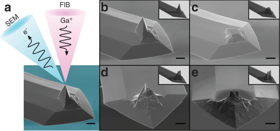 |
| a) Graphical illustration of simultaneous milling via FIB and imaging using SEM. b) Tapping-mode AFM tip prior to milling. c–e) Plateau, chisel, and double-tip. The asymmetry of these designs can be leveraged for the fabrication of highly complex patterns via mechanical nanolithography. Insets of Figures b–e correspond to graphical renderings of the probe geometry. Scale bars are 5 µm. (Reprinted from doi:10.1038/s41378-021-00300-y under a Creative Commons CC BY license) (click on image to enlarge) |
| "We focused on two novel types of asymmetric tips, which we termed 'chisel-tip' and 'double-tip', that show particular promise for nc-SPL," Farmakidis explains. "By controlling the writing angle, we show that the distance between the lines can be tuned to produce nanowires with sizes which vary from several nanometers to microns." |
| In their paper, the researchers demonstrate how, owing to the asymmetry of the chisel-tip probe, complex lithographic patterns of different dimensions can be produced, allowing for intricate patterns without scanning artifacts or resist buildup at the borders of the lithography path. |
| The double-tip configuration is suitable for nanopatterning applications down to and below 50 nm that require a nanoscale gap such as two conducting lines close to each other without overlap. |
| As the researchers point out, by using tips that do not necessarily have nanoscale dimensions themselves, they were able to pattern gaps that are effectively much smaller than the minimum probe dimensions. |
| They also note that patterns were produced at a speed of 20 µm/s and with the same tip, which showed no apparent wear after patterning. |
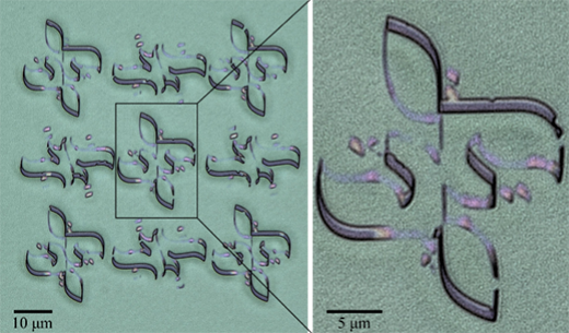 |
| Showcasing the capabilities of nc-SPL, Farmakidis collaborated with well-known calligraphy artist Majid Alyousef to reproduce complex calligraphic artwork in dimensions smaller than 100 times that of a human hair. (Image: University of Oxford) |
| The range of applications for nc-SPL are numerous. The technique can be used to achieve resolutions comparable or even better than state-of-the-art photolithography and charged beam lithography systems, which usually require multi-million dollar equipment. |
| Applications of this new fabrication technique include, but are not limited to, nanoelectronics including CMOS, organic and flexible nanoelectronics, devices based on 2D materials, as well as sensors employing sensitive reagents and biological materials (eg. proteins, DNA). Perhaps more importantly, it is an accessible tool to most researcher labs which can be used to harness and study the properties of nanostructures and nanomaterials. |
| "This was the first demonstration of something of this kind so there are naturally many directions we wish to explore," Farmakidis concludes. "One particularly exciting path is the implementation of the technique for sustainable nanomanufacturing. We are also exploring implementations in nanophotonics and metasurfaces." |
 By
Michael
Berger
– Michael is author of four books by the Royal Society of Chemistry:
Nano-Society: Pushing the Boundaries of Technology (2009),
Nanotechnology: The Future is Tiny (2016),
Nanoengineering: The Skills and Tools Making Technology Invisible (2019), and
Waste not! How Nanotechnologies Can Increase Efficiencies Throughout Society (2025)
Copyright ©
Nanowerk LLC
By
Michael
Berger
– Michael is author of four books by the Royal Society of Chemistry:
Nano-Society: Pushing the Boundaries of Technology (2009),
Nanotechnology: The Future is Tiny (2016),
Nanoengineering: The Skills and Tools Making Technology Invisible (2019), and
Waste not! How Nanotechnologies Can Increase Efficiencies Throughout Society (2025)
Copyright ©
Nanowerk LLC
|

Become a Spotlight guest author! Join our large and growing group of guest contributors. Have you just published a scientific paper or have other exciting developments to share with the nanotechnology community? Here is how to publish on nanowerk.com. |
